
Datasheet

- 18 -
Copyright 2011 National Semiconductor Corporation
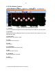
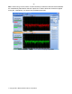
Config: This tab configures various features and modes of the ADC12D1X00RF and is shown
below. It accesses or changes the following functions, all of which are controlled through
Configuration Register 1.
Figure 11: Config Panel
• DPS – DDR Phase Select –
o In DDR, this determines the DDR Data-to-DCLK phase relationship. When unchecked,
the 0° Mode is selected. When checked the 90° Mode is selected.
o In SDR, when this box is unchecked data transitions on the Rising edge of DCLK and
when checked data transitions on the Falling edge of DCLK.
• OVS – Output Voltage Select – Selects the LVDS differential output voltage. When this is
unchecked, the reduced output amplitude is selected. When checked, the standard (higher)
output amplitude is used.
• TPM – Test Pattern Mode – When checked the device will continually output a fixed pattern on
the Data and OR outputs. When cleared, the normal ADC Data and OR information are output.
• PDI – Power down I Channel when checked.
• PDQ – Power down Q channel when checked.
• 2SC – Two’s Complement output mode is selected when checked. Default is offset binary.
• TSE – Check to enable Time Stamp feature.
• SDR – SDR mode when checked; DDR when unchecked. Default is DDR.
Note: Will only work in DDR mode, unless FPGA is changed.
Note: No changes will take effect until the Write Config Reg button is clicked.