
Datasheet

- 4 -
Copyright 2011 National Semiconductor Corporation
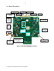
1.1 Features
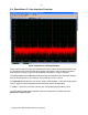
Demonstrates the ADC12D1X00RF's typical dynamic performance – see the datasheet
for full details.
Dual channel sample rates of up to 1.6/1.8 GS/s (limited by the ADC specifications and
the FPGA capture limitations)
Single channel (Interleaved) sample rates of up to 3.2/3.6 GS/s (limited by the ADC
specifications and the FPGA capture limitations)
FMC Expansion Header for streaming data capture
SMA I/O for easy AutoSync feature evaluation
External Hardware Trigger
Updated Status LEDs
On-board LMX2531 based clock circuit with a connector for a selectable external clock
A complete high-performance low-noise power management section for the ADC, clock
circuit, FPGA and USB controller
Single +7.5V power adapter input
Simplicity and performance of USB 2.0 connection to the PC
Functions with National's latest WaveVision 5 signal-path control and analysis software
1.2 Packing List
The ADC12D1X00RFRB kit consists of the following components:
• ADC12D1X00RFRB Board
• Documentation on CD Including
o ADC12D1X00RFRB Users Guide (this document)
o Wavevision 5 Software
o ADC12D1X00RFRB schematic & layout
o ADC12D1X00RFRB bill of materials
o ADC12D1X00RFRB performance plots
o FPGA source code
o Balun datasheets
• Hardware Kit Including
o 110V-240V AC to +7.5V DC Power Adapter
o USB cable
o 4 – DC blocks
o 2 – 50Ω terminators
o 1 – Anaren balun board (useful bandwidth of 400 MHz to 3 GHz)
o 1 – Mini-Circuits balun board (useful bandwidth of 4.5 MHz to 3 GHz)
o 4 – 6” SMA cables
1.3 References
• *ADC12D1X00RF datasheet
• *LMX2531 datasheet
• *Application Note 2132: Synchronizing Multiple GSPS ADCs in a System: The AutoSync Feature
*Note: Please refer to www.national.com for the latest edition of all datasheets / application notes.