
Datasheet


www.ti.com
Hardware
6.1 Microcontroller
The ADS1x31REF uses the MSP430F449 microcontroller. This device provides an LCD controller,
hardware SPI and UART interfaces, and a multiplier. The latter is important because the firmware must
perform many multiplications.
6.2 Power Supply
The ADS1x31REF operates from +5VDC and +3.3VDC. These supplies are generated by linear regulators
U1 and U2. Input power comes from either wall-adapter connector J2, or battery connector BT1. J2 is
switched; when a connector is plugged in, BT1 is disconnected.
Noise is important because the ADC voltage reference is typically taken from the power supply. The
supplies are heavily bypassed to reduce noise.
6.3 User Interface
The ADS1x31REF user interface consists of the display and switches SW2–5 and SW8. Switches are
connected to interrupt-capable GPIOs on the microcontroller, allowing them to wake the microcontroller
from sleep mode.
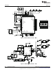
6.4 ADC Section
The ADC section consists of the installed ADS device itself and ancillary circuitry.
All signals on the installed ADS device are filtered by pass-through capacitors that help to reject
electromagnetic interference (EMI), radio frequency interference (RFI), and noise generated by the digital
circuitry.
6.4.1 Input Circuitry
The ADS1x31REF is designed to connect to resistive bridge sensors, particularly load cells. The input
channel is filtered by pass-through capacitors C38 and C39 and differential capacitor C7. Common-mode
capacitors C32 and C29 provide additional RF rejection.
6.4.2 Load Cell Header
The load cell header, J6, provides a convenient terminal for load cells having a properly fitted header
connector. It provides excitation and sense connections. The negative excitation line is connected to
ground through the installed ADS device. The ADS device conserves power by allowing excitation current
to flow only during conversion. See the ADS1131 data sheet or the ADS1231 data sheet for more
information.
The load cell connector’s pinout is given in Table 7. For connection examples, see Section 1.4.3 and
Section 1.4.4.
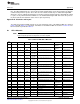
Table 7. Load Cell Header Pinout
PIN NO. PIN NAME FUNCTION
1 EXC+ Positive excitation; connected to +5VA
2 EXCSNS+ Positive sense; connected to external positive reference input
3 SIG+ Input for positive load cell output
4 SIG– Input for negative load cell output
5 EXCSNS– Negative sense; connected to external negative reference input
6 EXC– Negative excitation; connected to ground through installed ADS
device
21
SBAU175A–July 2010–Revised August 2011 ADS1131REF and ADS1231REF
Submit Documentation Feedback
Copyright © 2010–2011, Texas Instruments Incorporated