
Datasheet
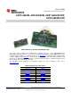

Analog Interface
www.ti.com
2 Analog Interface
For maximum flexibility, the ADS1246EVM is designed for easy interfacing to multiple analog sources.
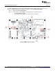
Samtec part numbers SSW-110-22-F-D-VS-K and TSM-110-01-T-DV-P provide a convenient 10-pin,
dual-row, header/socket combination at J8. This header/socket provides access to the analog input pins of
the ADS1246. Consult Samtec at http://www.samtec.com or call 1-800-SAMTEC-9 for a variety of mating
connector options. These signals can also be connected to the terminal block J4.
All of the pins on J4 and J8 are connected with minimal filtering or protection. Use appropriate caution
when handling these pins. Table 1 summarizes the pinouts for analog interfaces J4 and J8.
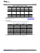
Table 1. J8/J4: Analog Interface Pinout
Pin Number Signal Description, ADS1146/ADS1246
J8.1, J4-2 A0(–) AINN
J8.2, J4-1 A0(+) AINP
J8.3-8 Unused —
J8.18 REF– External Reference source input
(– side of differential input)
J8.20 REF+ External Reference source input
(+ side of differential input)
J8.10-16 (even) Unused —
J8.15 Unused —
J8.9-19 (odd), J4-9 AGND Analog ground connections
(except J8.15)
3 Digital Interface
3.1 Serial Data Interface
The ADS1246EVM is designed to easily interface with multiple control platforms. Samtec part numbers
SSW-110-22-F-D-VS-K and TSM-110-01-T-DV-P provide a convenient 10-pin, dual-row, header/socket
combination at J7. This header/socket provides access to the digital control and serial data pins of the
ADC. Consult Samtec at http://www.samtec.com or call 1-800-SAMTEC-9 for a variety of mating
connector options.
All logic levels on J7 are 3.3V CMOS, except for the I
2
C™ pins. These pins conform to 3.3V I
2
C rules.
Table 2 describes the J7 serial interface pins.
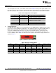
Table 2. J7: Serial Interface Pins
Pin No. Pin Name Signal Name I/O Type Pullup Function
J7.1 CNTL CS In High
J7.2 GPIO0 START In High
J7.3 CLKX SCLK In None ADS1246 SPI
clock
J7.4 DGND DGND In/Out None Digital ground
J7.5 CLKR Unused — None
J7.6 GPIO1 MR In High Master reset
J7.7 FSX Unused — None
J7.8 GPIO2 Unused — None
J7.9 FSR DRDY Out None
J7.10 DGND DGND In/Out None Digital ground
J7.11 DX DIN In None ADS1246 SPI
data in
J7.12 GPIO3 PWRSEL In High Selects ±2.5V
or +5V supply
4
ADS1146EVM, ADS1246EVM, ADS1146EVM-PDK, ADS1246EVM-PDK SBAU149B–June 2009–Revised May 2011
Submit Documentation Feedback
Copyright © 2009–2011, Texas Instruments Incorporated