
Datasheet

www.ti.com
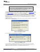
Power Supplies
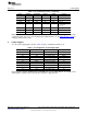
Table 2. J7: Serial Interface Pins (continued)
Pin No. Pin Name Signal Name I/O Type Pullup Function
J7.13 DR DOUT/DRDY Out None ADS1247 data out
J7.14 GPIO4 Unused -— None
J7.15 INT DRDY Out None
J7.16 SCL SCL I
2
C High I
2
C clock
J7.17 TOUT CLK In None Can be used to provide
a clock from a
processor
J7.18 DGND DGND In/Out None Digital ground
J7.19 GPIO5 CLK Select — None
J7.20 SDA SDA I
2
C High I
2
C data
Many pins on J7 have weak pull-up resistors. These resistors provide default settings for many of the
control pins. Many pins on J7 correspond directly to ADS1247 pins. See the ADS1247 data sheet for
complete details on these pins.
4 Power Supplies
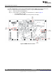
J3 is the power-supply input connector. Table 3 lists the configuration details for J3.
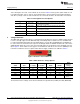
Table 3. J3 Configuration: Power-Supply Input
Pin No. Pin Name Function Required
J3 .1 +VA Unused No
J3 .2 –VA Unused No
J3.3 +5VA +5V analog supply Always
J3.4 –5VA –5V analog supply Only in bipolar mode
J3.5 DGND Digital ground input Yes
J3.6 AGND Analog ground input Yes
J3.7 +1.8VD 1.8V digital supply No
J3.8 VD1 Unused No
J3.9 +3.3VD 3.3V digital supply Always
J3.10 +5VD +5V digital supply No
All of the power supplies (AVDD, AVSS, and DVDD) have corresponding jumpers on J10 that can be
replaced with a current meter to measure the respective supply currents.
5
SBAU148B– June 2009– Revised May 2011 ADS1147EVM, ADS1247EVM, ADS1147EVM-PDK, ADS1247EVM-PDK
Submit Documentation Feedback
Copyright © 2009–2011, Texas Instruments Incorporated