User's Guide SBAU142B – April 2009 – Revised May 2011 ADS1148EVM, ADS1248EVM, ADS1148EVM-PDK, and ADS1248EVM-PDK ADS1248EVM (Left) and ADS1248EVM-PDK (Right) This user's guide describes the characteristics, operation, and use of the ADS1148EVM and ADS1248EVM, both by themselves and as part of the ADS1148EVM-PDK or ADS1248EVM-PDK.
www.ti.com 1 2 3 4 5 6 7 8 9 10 Contents EVM Overview ............................................................................................................... 3 Analog Interface ............................................................................................................. 3 Digital Interface .............................................................................................................. 4 Power Supplies ...................................................................
EVM Overview www.ti.com 1 EVM Overview 1.1 Features ADS1148EVM/ADS1248EVM Features: • Contains all support circuitry needed for the ADS1148/ADS1248 • ±2.
Digital Interface www.ti.com All of the pins on J4 and J8 are connected with minimal filtering or protection. Use appropriate caution when handling these pins. Table 1 summarizes the pinouts for analog interfaces J4 and J8. Table 1. J8/J4: Analog Interface Pinout Pin Number Signal Description, ADS1148/ADS1248 J8.1, J4-1 A0(–) AIN0 J8.2, J4-2 A0(+) AIN1 J8.3, J4-3 A1(–) AIN2 J8.4, J4-4 A1(+) AIN3 J8.5, J4-5 A2(–) AIN4 J8.6, J4-6 A2(+) AIN5 J8.7, J4-7 A3(–) AIN6 J8.
Power Supplies www.ti.com Table 2. J7: Serial Interface Pins (continued) Pin No. Pin Name Signal Name I/O Type Pullup J7.16 SCL SCL I2C High I2C clock Function J7.17 TOUT CLK In None Can be used to provide a clock from a processor J7.18 DGND DGND In/Out None Digital ground J7.19 GPIO5 CLK Select – None J7.20 SDA SDA I2C High I2C data Many pins on J7 have weak pull-up resistors. These resistors provide default settings for many of the control pins.
Voltage Reference 5 www.ti.com Voltage Reference The ADS1248 device has the option of selecting between three different references: REF0, REF1, and the internal reference, through registers in the ADS1248 chip. The EVM provides a 2.048V reference for REF1 from U1, filtered and buffered through U2. This 2.048V may be used to drive the REF1P input. REF1P should not be connected to AVDD through switch S1 because this connection will violate the specification for the maximum reference input.
EVM Operation www.ti.com 6.2 Usage as a Stand-Alone EVM If using the EVM in your own system and not with the PDK hardware and software, observe the following recommendations: • J13 should be removed if the external clock source is used and the TOUT pin is still driven by a processor in order to avoid conflicts. • Jumper J2 can be used to always select the U8 oscillator (DVDD position) or allow the onboard/external clock selection to be controlled by GPIO5 (J7.19) as shown in Figure 2. Figure 2.
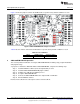
ADS1248EVM-PDK Kit Operation 7.3 www.ti.com Default Jumper Settings and Switch Positions Figure 3 shows the jumpers found on the EVM and the respective factory default conditions for each. Figure 3. ADS1248EVM Default Jumper Locations Table 6 lists the switches found on the EVM and the respective factory default conditions for each. Table 6.
ADS1248EVM-PDK Kit Operation www.ti.com 8.1 Installing the ADCPro Software CAUTION Do not connect the ADS1248EVM-PDK before installing the software on a suitable PC. Failure to observe this caution may cause Microsoft Windows to not recognize the ADS1248EVM-PDK as a connected device. The CD-ROM shipped with the ADS1248EVM contains an installer for ADCPro as well as an installer for the ADS1248EVM plug-in. The latest software is available from the TI website at http://www.ti.com/.
ADS1248EVM-PDK Kit Operation 8.2 www.ti.com Setting Up the ADS1248EVM-PDK The ADS1248EVM-PDK contains both the ADS1248EVM and the MMB3 motherboard; however, the devices are shipped unconnected. Follow these steps to set up the ADS1248EVM-PDK. Step 1. Unpack the ADS1248EVM-PDK kit. Step 2. Set the switches on the MMB3 as described below, as shown in Figure 6. • Set switch SW4 to the right. • Set the DAC switch (SW5) to the OUT position (to the right). Figure 6. MMB3 Switch Locations Step 3.
ADS1248EVM-PDK Kit Operation www.ti.com Figure 7. Connecting ADS1248EVM to MMB3 CAUTION Do not misalign the pins when plugging the ADS1248EVM into the MMB3. Check the pin alignment carefully before applying power to the PDK. Step 4. 8.2.1 Set the jumpers and switches on the ADS1248EVM as shown in Figure 3 (note that these settings are the factory-configured settings for the EVM). About the MMB3 The MMB3 is a Modular EVM System motherboard.
ADS1248EVM-PDK Kit Operation www.ti.com USB USB RESET +5VA -5VA +5VD PWR & VREF +3.3V +1.8V +10V TUSB3410 -10V Supplied to Daughtercard Power Connector LCD DISPLAY 2.5V OPER BSL +1 DAC1220 MSP430F449 RESET -1 DAC IN OUT Analog Daughtercard Modular Connectors Serial Power Joystick Power from PWR & VREF Block Figure 8. MMB3 Block Diagram The MMB3 was designed to be used as a stand-alone demonstration platform for low-speed data converters.
ADS1248EVM-PDK Kit Operation www.ti.com The program currently runs only on Microsoft Windows platforms of Windows XP; Windows Vista is NOT supported. If this is the first time installing ADCPro and plug-ins, follow these procedures to run ADCPro and perform any necessary firmware installations. Make sure the ADCPro software and device plug-in software are installed from the CD-ROM as described in Section 8.1, Installing the ADCPro Software. Step 1.
ADS1248EVM-PDK Kit Operation break Step 2. www.ti.com Select ADS1248EVM from the EVM drop-down menu. The ADS1248EVM-PDK plug-in appears in the left pane, as shown in Figure 10. Figure 10. ADS1248EVM-PDK Plug-In Display Window Step 3. 14 The ADS1248EVM-PDK plug-in window has a status area at the top of the screen. When the plug-in is first loaded, the plug-in searches for the board. You will see a series of messages in the status area indicating this action.
ADS1248EVM-PDK Kit Operation www.ti.com break Step 4. If the plug-in cannot connect to the EVM, you will see a window as shown in Figure 11. This message may indicate that the firmware is not loaded on the MMB3. You may select Retry Auto Connect; if that action fails, select Retry Manual Connect and specify the COM port to be used. Figure 11. Connection Timeout Step 5. The plug-in detects whether or not the board has the correct firmware loaded.
ADS1248EVM-PDK Kit Operation www.ti.com Switch the BSL switch (SW4) on the MMB3 to the BSL position (to the left) as instructed, then press OK. The plug-in will download the firmware to the MMB3. This operation may take a couple of minutes, so the progress is updated in the message at the top of the ADS1248 plug-in window (as Figure 13 shows). The firmware is saved in flash memory on the MMB3, so this operation should only need to be performed once. Figure 13.
Evaluating Performance with the ADCPro Software www.ti.com When the firmware download completes, the message box shown in Figure 14 appears. Follow the on-screen instructions and the plug-in should now connect to the EVM. Figure 14. Firmware Download Complete Message Box 9 Evaluating Performance with the ADCPro Software The evaluation software is based on ADCPro, a program that operates using a variety of plug-ins. To use ADCPro, load an EVM plug-in and a test plug-in.
Evaluating Performance with the ADCPro Software 9.1.1 www.ti.com I/O Config Tab This tab is the primary tab that controls the function of the multiplexer in the ADS1248. Recall that the ADS1248 multiplexer is configured as shown in Figure 15. By default, all channels are set as analog inputs; the IDACs are not routed to any channel and the IDAC controls are disabled. These controls are enabled when the correct IDAC settings are made on the Power & Ref tab (see Section 9.1.3).
www.ti.com Evaluating Performance with the ADCPro Software Input pins AIN2-AIN7 can be selected to be an analog input or GPIO. If an input is to be used as a GPIO, check the GPIO box as shown in Figure 16. Figure 16. I/O Config Tab When an input is selected as a GPIO, its label turns green and the IDAC controls for that channel are disabled.
Evaluating Performance with the ADCPro Software www.ti.com Each input channel can also have a VBIAS applied to it. Checking the VBIAS box on a channel applies the VBIAS voltage, which is approximately half the value of the supply. You can test this option as shown in Figure 17, using one channel tied to a value close to ground (make sure you observe the common-mode restrictions listed in the ADS1248 product data sheet) as a reference for this signal. Figure 17.
www.ti.com 9.1.2 Evaluating Performance with the ADCPro Software GPIO Tab When an input is selected to be a GPIO, its controls are enabled on the GPIO tab, shown in Figure 18. By default, the GPIOs are enabled as inputs. Pressing the Input button reads the state of the enabled inputs; if the input is high, the corresponding light turns green. Figure 18.
Evaluating Performance with the ADCPro Software www.ti.com To make the GPIO an output, the toggle switch can be switched to output mode, as shown in Figure 19. Figure 19.
www.ti.com Evaluating Performance with the ADCPro Software With the GPIO configured as an output, the pushbutton switch controls the state of the output pin. When pressed (as illustrated in Figure 20), the button lights up and the GPIO is set to a high state; when the switch is dark (as Figure 19 shows), the GPIO is in a low state. Figure 20.
Evaluating Performance with the ADCPro Software 9.1.3 www.ti.com Power & Ref Tab The Power & Ref tab is shown in Figure 21. This tab controls the selection of the power-supply mode, reference sources, and IDACs. Figure 21. Power & Ref Tab Note that with the Internal Reference off, the IDAC controls are disabled, because the IDACs cannot be used unless the internal reference is turned on.
www.ti.com Evaluating Performance with the ADCPro Software The Power Supply control selects between single supply (+5V) mode and bipolar supply (±2.5V) mode. The EVM draws its supply voltages from the MMB3 motherboard, and has onboard circuitry to select between the +5V and bipolar supplies. The Reference Select control selects between VREF0, VREF1, and the Internal Reference. When VREF1 is selected, the VREF value is set to 2.048V, with switch S1 set to BUFF.
Evaluating Performance with the ADCPro Software 9.1.4 www.ti.com Cal Tab The Cal tab (Figure 22) controls the calibration functions of the ADS1248. Figure 22. Cal Tab Pressing the Self Offset Calibrate button causes the ADS1248 to perform a self calibration; the offset and full-scale register values are then updated on the plug-in screen. You may also write to these registers by typing in hex values in the New fields, then press the Set button.
www.ti.com 9.1.5 Evaluating Performance with the ADCPro Software About Tab The About tab displays information about the EVM and software, as shown in Figure 23. Figure 23. About Tab The Plugin Version and Firmware Version indicators show the version numbers of the plug-in and firmware code, respectively. The ID indicator shows the value of the ID [3:0] bits in the ADS1248 ID register. The Notes indicator may show relevant notes about the plug-in or firmware code, if there are any.
Evaluating Performance with the ADCPro Software 9.1.6 www.ti.com Collecting Data Once you have configured the ADS1248 for your test scenario, press the ADCPro Acquire button to start the collection of the number of datapoints specified in the Test plug-in Block Size control. The ADS1248EVM-PDK plug-in disables all the front panel controls while acquiring, and displays a progress bar as shown in Figure 24. Figure 24.
Schematics and Layout www.ti.com 9.2 Troubleshooting If the ADS1248EVM plug-in cannot find the ADS1248EVM-PDK, press the USB RESET button on the MMB3 (refer to Figure 6) and try again. If ADCPro stops responding while the ADS1248EVM-PDK is connected, try unplugging the USB cable from the PDK. Unload and reload the plug-in before reapplying power to the PDK. 10 Schematics and Layout Schematics for the ADS1148EVM and ADS1248EVM are appended to this user's guide.
Revision History www.ti.com Table 7. ADS1148EVM/ADS1248EVM Bill of Materials (continued) Item No.
1 2 3 4 5 150nF 7 1 8 1 2 3 TP2 REFP D5 FRC_BAT54 0.1uF DVDD U2 2 R1 10K C1 1uF VIN TEMP GND 4 VOUT TRIM 6 C4 22uF 5 47 C5 22uF C36 C16 10uF D6 FRC_BAT54 C34 U1 2 3 4 S1 R3 6 OPA227 3 APPROVED RA1A 100K AVDD C6 +5V ENGINEERING CHANGE NUMBER C14 +5V D REV DVDD 2K J1 JPR-1X3 6 REVISION HISTORY R2 D 0.1uF U12 5 0.1uF C15 0.1uF -5V R14 0 TP1 AVSS R15 0 C20 REF5020ID 4 VDD RESET CT GND MR 1 2 3 TPS3836DBV 10uF TP3 Int REF 1 47 R12 47 9 B 3 C10 0.
1 2 3 4 5 REV DVDD 2K J1 JPR-1X3 6 REVISION HISTORY R2 ENGINEERING CHANGE NUMBER APPROVED C14 RA1A 100K AVDD 150nF +5V 7 1 8 1 2 3 C6 TP2 D5 REFP FRC_BAT54 0.1uF U2 2 D R1 +5V 10K C1 1uF VIN TEMP GND 4 VOUT TRIM 6 C4 22uF 5 47 C5 22uF D 0.1uF D6 FRC_BAT54 C34 U1 2 3 4 R3 6 OPA227 3 DVDD C36 U12 5 0.1uF C15 0.1uF -5V 4 TP1 AVSS C20 R14 REF5020ID 0 C16 10uF R15 VDD RESET CT GND MR 1 2 3 TPS3836DBV 0 10uF TP3 Int REF 1 22 1 47 R12 47 9 B 3 C10 0.
Evaluation Board/Kit Important Notice Texas Instruments (TI) provides the enclosed product(s) under the following conditions: This evaluation board/kit is intended for use for ENGINEERING DEVELOPMENT, DEMONSTRATION, OR EVALUATION PURPOSES ONLY and is not considered by TI to be a finished end-product fit for general consumer use. Persons handling the product(s) must have electronics training and observe good engineering practice standards.
IMPORTANT NOTICE Texas Instruments Incorporated and its subsidiaries (TI) reserve the right to make corrections, modifications, enhancements, improvements, and other changes to its products and services at any time and to discontinue any product or service without notice. Customers should obtain the latest relevant information before placing orders and should verify that such information is current and complete.