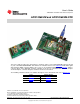
User's Guide SBAU090C – November 2003 – Revised July 2010 ADS1256EVM and ADS1256EVM-PDK This user's guide describes the characteristics, operation, and use of the ADS1256EVM, both by itself and as part of the ADS1256EVM-PDK. This EVM is an evaluation fixture for the ADS1256 24-bit delta-sigma (ΔΣ) analog-to-digital converter (ADC). It also serves as an evaluation platform for the ADS1255, which is a proper subset of the ADS1256. It allows evaluation of all aspects of the ADS1256 device.
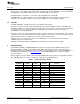
www.ti.com 1 2 3 4 5 6 7 8 9 10 Contents EVM Overview ............................................................................................................... 3 Analog Interface ............................................................................................................. 5 Digital Interface .............................................................................................................. 6 Power Supplies ...................................................................
EVM Overview www.ti.com 37 38 39 40 .................................................................................. ADS1256EVM PCB: Layer 1 ............................................................................................. ADS1256EVM PCB: Layer 2 ............................................................................................. ADS1256EVM PCB: Bottom-Side Image ..............................................................................
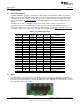
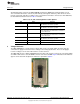
EVM Overview 1.2 www.ti.com Introduction The ADS1256EVM, shown in Figure 1, is an evaluation module built to the TI Modular EVM System specification. It can be connected to any Modular EVM System interface card. The ADS1256EVM is available as a stand-alone printed circuit board (PCB) or as part of the ADS1256EVM-PDK, which includes an MMB0 motherboard and software. As a stand-alone PCB, the ADS1256EVM is useful for prototyping designs and firmware.
Analog Interface www.ti.com The power connector (J3) carries the power supplies. The ADS1256EVM requires a +5V analog supply and a +1.8V to +3.3V digital supply. The board is designed using a single ground net connected to DGND. An AGND pin is also provided. Power options are routed through J4, J9, and J10. The GPIO header (J5) provides a connection to the four GPIO pins on the EVM. The ADS1256 uses separate supplies for its analog and digital sections. A jumper is inserted in each supply line.
Digital Interface www.ti.com 3 Digital Interface 3.1 Serial Data Interface The ADS1256EVM is designed to easily interface with multiple control platforms. Samtec part numbers SSW-110-22-F-D-VS-K and TSM-110-01-T-DV-P provide a convenient 10-pin, dual-row, header/socket combination at J2. This header/socket provides access to the digital control and serial data pins of the TSC. Consult Samtec at www.samtec.com or call 1-800-SAMTEC-9 for a variety of mating connector options.
Power Supplies www.ti.com Each pin is connected to the GPIO header through a 100Ω resistor. 100kΩ pull-downs on each pin protect the GPIOs when they are configured as inputs, which is the default setting. The GPIO header, J5, carries the GPIO pins for the ADS1256. The GPIO header pinout is described in Table 3. Table 3.
Power Supplies 4.1 www.ti.com Power Options There are six jumpers on the ADS1256EVM, arranged in a single jumper block of seven rows, each of which can be shorted. (In the schematic, J4, J9, and J10 are all combined to make this single block). The pinout of this jumper block is shown in Figure 3. Figure 3. Jumper Block J4 connects AVDD from the +5V from the power-supply header, J3. J4 also connects the DVDD supply to the ADS1256 device. DVDD can be set to 1.8V with J9, or to 3.
Voltage Reference www.ti.com 4.1.6 J10 Pins 5-6: AGND Select Shorting this jumper connects the ADS1256EVM ground net to AGND. For normal operation, J4.1-2, J4.3-4, and J4.9-10 must be connected (either directly or through an ammeter); either J4.5-6 or J4.7-8 must be connected, and either (or both) of J4.11-12 and J4.13-14 must be connected, as well. Otherwise, the board will not function. Refer to Table 5 for details. Table 5.
Clock Source www.ti.com Table 6. Reference Input Select Switch Board Marking Switch Position Input Source VRP Connection EST Down External J1.20 VRN Connection J1.18 OBH Middle Onboard, high common-mode AVDD +2.5V OBL Up Onboard, low common-mode +2.5V AGND In the EXT position, J1 pins 18 and 20 are connected to the ADS1256 reference input.
EVM Operation www.ti.com 7 EVM Operation This section provides information on the analog input, digital control, and general operating conditions of the ADS1256EVM. 7.1 Analog Input The analog input sources can be applied directly to J1 (top or bottom side). Additionally, switches S1 and S2 must be set to route the input signals from J1. Otherwise, the inputs are used to measure the reference or inputs shorted to the reference. Switches S1 and S2 are shown in Figure 6. Figure 6. Switches S1 and S2 7.
EVM Operation 7.1.2 www.ti.com S2: AIN2-3 Input Select These switches control which lines are routed to the ADS1256 AIN2 through AIN3 inputs. The positions of the switches are described in Table 9. Table 9. AIN2-3 Input Select Switch (S2) Board Marking Switch Position Input Source AIN0 Connection EXT Left External J1.4 AIN1 Connection J1.3 REF Middle Reference voltage +2.5V AGND ZERO Right Zero (shorted to reference) +2.5V +2.
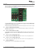
EVM Operation www.ti.com 7.4 Default Jumper Settings and Switch Positions Figure 7 shows the jumpers and switches found on the EVM and the respective factory default conditions for each. Figure 7. ADS1256EVM Default Jumper and Switch Locations The jumpers on J4 provide a convenient way to measure the current for any of the power-supply currents AVDD (analog +V power), DVDD (digital power), AVSS (analog –V power), or the ground connections VGND and DGND.
ADS1256EVM-PDK Kit Operation www.ti.com Table 11. Default Switch Positions 8 Switch Default Position S1 Left AIN0-1 Input Select Switch Switch Description S2 Left AIN2-3 Input Select Switch S3 Up Reference Input Select S4 Left System Clock Select Switch ADS1256EVM-PDK Kit Operation This section provides information on using the ADS1256EVM-PDK, including setup, program installation, and program usage.
ADS1256EVM-PDK Kit Operation www.ti.com Figure 8. ADS1256EVM-PDK Setup Wizard Figure 9.
ADS1256EVM-PDK Kit Operation www.ti.com Figure 10. ADS1256EVM-PDK Installation in Progress Figure 11.
ADS1256EVM-PDK Kit Operation www.ti.com The software should now be installed, but the USB drivers may not yet have been loaded by the PC operating system. This step completes when the ADCPro software is executed; see Section 8.4, Running the Software and Completing Driver Installation. 8.2 Setting Up the ADS1256EVM-PDK The ADS1256EVM-PDK contains both the ADS1256EVM and the MMB0 motherboard; however, these devices are shipped unconnected. Follow these steps to set up the ADS1256EVM-PDK: Step 1.
ADS1256EVM-PDK Kit Operation space Step 3. www.ti.com Plug the ADS1256EVM into the MMB0. CAUTION Do not misalign the pins when plugging the ADS1256EVM into the MMB0. Check the pin alignment carefully before applying power to the PDK. Step 4. Set the jumpers and switches on the ADS1256EVM as shown in Figure 13 (note that these settings are the factory-configured settings for the EVM): • Set jumper block J4 as shown in Figure 7. • Set the reference source select switches S1 and S2 to the center position.
ADS1256EVM-PDK Kit Operation www.ti.com 8.2.1 About the MMB0 The MMB0 is a Modular EVM System motherboard. It is designed around the TMS320VC5507, a DSP from Texas Instruments that has an onboard USB interface. The MMB0 also has 16MB of SDRAM installed. The MMB0 is not sold as a DSP development board, and it is not available separately. TI cannot offer support for the MMB0 except as part of an EVM kit. For schematics or other information about the MMB0, contact Texas Instruments. 8.
ADS1256EVM-PDK Kit Operation 8.3.2 www.ti.com Connecting a Laboratory Power Supply A laboratory power supply can be connected through terminal block J14 on the MMB0, as shown in Figure 15. Both unipolar and bipolar configurations are supported. To • • • use a unipolar lab power supply configuration: Disconnect J12 on the MMB0. Connect a +5V dc supply to the +5VD terminal on J14. Connect ground of the dc supply to the GND terminal on J14.
ADS1256EVM-PDK Kit Operation www.ti.com 8.4.1 NI-VISA USB Device Driver Installation 1. After the ADCPro software is installed, apply power to the PDK and connect the board to an available PC USB port. 2. The computer should recognize new hardware and begin installing the drivers for the hardware. Figure 16 through Figure 19 are provided for reference to show the installation steps.
ADS1256EVM-PDK Kit Operation www.ti.com Figure 18. NI-VISA Driver Installation Wizard, Screen 3 Figure 19.
ADS1256EVM-PDK Kit Operation www.ti.com This should complete the installation of the NI-VISA drivers. You can verify proper installation by opening the Device Manager and locating the drivers as shown in Figure 20. Figure 20. NI-VISA Driver Verification Using Device Manager 8.4.2 USBStyx Driver Installation 1. Start the software by selecting ADCPro from the Windows Start menu. The screen shown in Figure 21 appears. Figure 21.
ADS1256EVM-PDK Kit Operation www.ti.com space 2. Select ADS1256EVM from the EVM drop-down menu. The ADS1256EVM-PDK plug-in appears in the left pane, as Figure 22 shows. Figure 22. ADS1256EVM-PDK Plug-In Display Window 3. The ADS1256EVM-PDK plug-in window has a status area at the top of the screen. When the plug-in is first loaded, the plug-in searches for the board. You will see a series of messages in the status area indicating this action. 4.
ADS1256EVM-PDK Kit Operation www.ti.com Figure 23. Install New Driver Wizard Screen 1 Figure 24.
ADS1256EVM-PDK Kit Operation www.ti.com Figure 25. Install New Driver Wizard Screen 3 Figure 26.
ADS1256EVM-PDK Kit Operation www.ti.com Figure 27. Install New Driver Wizard Screen 5 5. Once Windows finishes installing the software driver, the plug-in downloads the firmware to the MMB0. The status area will display Connected to EVM when the device is connected and ready to use. If the firmware does not load properly, you can try resetting the MMB0 by pressing Reset and then reloading the plug-in. Verify the proper installation of the USBStyx driver using the Device Manager.
Evaluating Performance with the ADCPro Software 9 www.ti.com Evaluating Performance with the ADCPro Software The evaluation software is based on ADCPro, a program that operates using a variety of plug-ins. (The ADS1256EVM plug-in is installed as described in the installation section, Section 8.) To use ADCPro, load an EVM plug-in and a test plug-in. To load an EVM plug-in, select it from the EVM menu. To load a test plug-in, select it from the Test menu.
Evaluating Performance with the ADCPro Software www.ti.com 9.1.1 MUX Tab The first tab of the ADS1256EVM plug-in is the MUX tab. In the tab, two columns of push buttons are used to select the positive and negative inputs for ADS1256. This selection, combined with switches S1 and S2, selects the measurement for the inputs applied to the analog interface J1. The MUX tab is shown in Figure 30. Figure 30.
Evaluating Performance with the ADCPro Software 9.1.2 www.ti.com Clocks Tab The next tab is the Clocks tab, as shown in Figure 31. This tab controls the master clock of the ADS1256EVM. Enter the master clock frequency in the Clock In window. The clock source can be selected from between the EVM onboard crystal and the MMB0. The DO/CLKOUT rate can be set by the Clock Out Rate pull-down menu. There are options to set CLKOUT to fCLKIN, fCLKIN/2, fCLKIN/4, or to turn it off. Figure 31.
Evaluating Performance with the ADCPro Software www.ti.com 9.1.3 GPIO Tab The GPIO tab is used to control the GPIO pins (D0 through D3) on the ADS1256. Four switches are used to select the GPIO mode (input or output). If the pin is selected as an output, a push button is used to set the output to be either high or low. If the pin is selected as an input, the Read Inputs button read the inputs and an indicator light shows if the input is high or low. Figure 32 illustrates the GPIO tab. Figure 32.
Evaluating Performance with the ADCPro Software 9.1.4 www.ti.com Power and Reference Tab The Power & Ref tab selects the reference input, the sensor detect magnitude, and the standby condition. The VREF Source window has three pushbuttons that select the reference source and should correspond with the reference setting for switch S3. OBL sets the reference input from AGND to VREF, while OBH sets the reference input from VREF to AVDD. External sets the input from VREF– to VREF+ on the analog input header.
Evaluating Performance with the ADCPro Software www.ti.com 9.1.5 Calibration Tab The Cal tab (as Figure 34 illustrates) controls the calibration of the offset and gain error of the ADS1256. Pressing a pushbutton at the top of the tab runs a self-calibration of the device. Four buttons allow four other calibration options: Self Offset Calibration, System Offset Calibration, Self Gain Calibration, and System Gain Calibration.
Evaluating Performance with the ADCPro Software 9.1.6 www.ti.com About Tab The About tab displays information about the EVM and software, as Figure 35 shows. The Plugin Version and Firmware Version indicators show the version numbers of the plug-in and firmware code, respectively. The Notes indicator may show relevant notes about the plug-in or firmware code, if there are any. Figure 35.
Evaluating Performance with the ADCPro Software www.ti.com 9.1.7 Collecting Data Once you have configured the ADS1256 for your test scenario, pressing the ADCPro Acquire button starts the collection of the number of datapoints specified in the Test plug-in Block Size control. The ADS1256EVM-PDK plug-in disables all the front panel controls while acquiring, and displays a progress bar as shown in Figure 36. Figure 36.
Schematics and Layout 10 www.ti.com Schematics and Layout A schematic for the ADS1256EVM is appended to this user's guide. The bill of materials is provided in Table 12. Figure 37 through Figure 40 illustrate the ADS1256EVM printed circuit board (PCB) layouts. Table 12.
Schematics and Layout www.ti.com Figure 37. ADS1256EVM PCB: Top-Side Image Figure 38. ADS1256EVM PCB: Layer 1 Figure 39. ADS1256EVM PCB: Layer 2 Figure 40.
1 2 3 4 REVISION HISTORY S1 ESW_EG2305A REV C1 10nF ENGINEERING CHANGE NUMBER APPROVED C14 DNP D J7 RESET R3 DVDD J1 AN0AN1AN2AN3AGND AGND AGND VCOM AGND AGND C9 DNP 2 4 6 8 10 12 14 16 18 20 AN0+ AN1+ AN2+ AN3+ AN4+ AN5+ AN6+ AN7+ REFREF+ C10 C11 DNP AVDD ANALOGHDR 0.1uF C23 2 R1 0.1uF VIN VOUT TEMP GND TRIM 3 6 5 S4 CNTL CLKX CLKR FSX FSR DX DR INT TOUT GPIO5 NKK_SS12SDP2 RA3 J5 D0C D1C D2C D3C 100 X1 7.
Evaluation Board/Kit Important Notice Texas Instruments (TI) provides the enclosed product(s) under the following conditions: This evaluation board/kit is intended for use for ENGINEERING DEVELOPMENT, DEMONSTRATION, OR EVALUATION PURPOSES ONLY and is not considered by TI to be a finished end-product fit for general consumer use. Persons handling the product(s) must have electronics training and observe good engineering practice standards.
IMPORTANT NOTICE Texas Instruments Incorporated and its subsidiaries (TI) reserve the right to make corrections, modifications, enhancements, improvements, and other changes to its products and services at any time and to discontinue any product or service without notice. Customers should obtain the latest relevant information before placing orders and should verify that such information is current and complete.