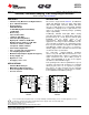
ADS1274 ADS1278 SBAS367F – JUNE 2007 – REVISED FEBRUARY 2011 www.ti.com Quad/Octal, Simultaneous Sampling, 24-Bit Analog-to-Digital Converters Check for Samples: ADS1274, ADS1278 FEATURES DESCRIPTION • Simultaneously Measure Four/Eight Channels • Up to 144kSPS Data Rate • AC Performance: 70kHz Bandwidth 111dB SNR (High-Resolution Mode) –108dB THD • DC Accuracy: 0.8μV/°C Offset Drift 1.
ADS1274 ADS1278 SBAS367F – JUNE 2007 – REVISED FEBRUARY 2011 www.ti.com This integrated circuit can be damaged by ESD. Texas Instruments recommends that all integrated circuits be handled with appropriate precautions. Failure to observe proper handling and installation procedures can cause damage. ESD damage can range from subtle performance degradation to complete device failure.
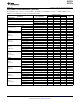
ADS1274 ADS1278 SBAS367F – JUNE 2007 – REVISED FEBRUARY 2011 www.ti.com ELECTRICAL CHARACTERISTICS All specifications at TA = –40°C to +105°C, AVDD = +5V, DVDD = +1.8V, IOVDD = +3.3V, fCLK = 27MHz, VREFP = 2.5V, VREFN = 0V, and all channels active, unless otherwise noted.
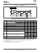
ADS1274 ADS1278 SBAS367F – JUNE 2007 – REVISED FEBRUARY 2011 www.ti.com ELECTRICAL CHARACTERISTICS (continued) All specifications at TA = –40°C to +105°C, AVDD = +5V, DVDD = +1.8V, IOVDD = +3.3V, fCLK = 27MHz, VREFP = 2.5V, VREFN = 0V, and all channels active, unless otherwise noted. ADS1274, ADS1278 PARAMETER TEST CONDITIONS MIN TYP MAX UNIT AC PERFORMANCE f = 1kHz, –0.5dBFS (5) Crosstalk High-Speed mode Signal-to-noise ratio (SNR) (6) (unweighted) High-Resolution mode VREF = 2.
ADS1274 ADS1278 SBAS367F – JUNE 2007 – REVISED FEBRUARY 2011 www.ti.com ELECTRICAL CHARACTERISTICS (continued) All specifications at TA = –40°C to +105°C, AVDD = +5V, DVDD = +1.8V, IOVDD = +3.3V, fCLK = 27MHz, VREFP = 2.5V, VREFN = 0V, and all channels active, unless otherwise noted. ADS1274, ADS1278 PARAMETER TEST CONDITIONS MIN TYP MAX UNIT POWER SUPPLY AVDD DVDD (9) 4.75 5 5.25 V 0.1 ≤ fCLK ≤ 32.768MHz 1.65 1.8 1.95 V 32.768MHz < fCLK ≤ 37MHz 2.0 2.1 2.
ADS1274 ADS1278 SBAS367F – JUNE 2007 – REVISED FEBRUARY 2011 www.ti.
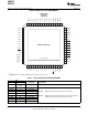
ADS1274 ADS1278 SBAS367F – JUNE 2007 – REVISED FEBRUARY 2011 www.ti.com Table 1. ADS1274/ADS1278 PIN DESCRIPTIONS (continued) PIN NAME NO. FUNCTION DESCRIPTION AINN1 4 Analog input AINN2 2 Analog input AINN3 64 Analog input AINN4 62 Analog input AINN5 52 Analog input AINN6 50 Analog input AINN7 48 Analog input AINN8 46 Analog input AVDD 5, 44, 53, 60 Analog power supply VCOM 55 Analog output VREFN 57 Analog input Negative reference input.
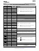
ADS1274 ADS1278 SBAS367F – JUNE 2007 – REVISED FEBRUARY 2011 www.ti.com SPI FORMAT TIMING tCLK tCPW CLK · · · tCPW tCD tCONV DRDY tSD tDS tSCLK tSPW SCLK tSPW tMSBPD DOUT Bit 23 (MSB) tDOPD tDOHD Bit 22 tDIST Bit 21 tDIHD DIN SPI FORMAT TIMING SPECIFICATION For TA = –40°C to +105°C, IOVDD = 1.65V to 3.6V, and DVDD = 1.65V to 1.95V, unless otherwise noted.
ADS1274 ADS1278 SBAS367F – JUNE 2007 – REVISED FEBRUARY 2011 www.ti.com FRAME-SYNC FORMAT TIMING tCPW tCLK CLK tCPW tCS tFRAME tFPW tFPW FSYNC tFS tSCLK tSPW tSF SCLK tSPW tMSBPD DOUT tDOHD Bit 23 (MSB) Bit 22 tDIST tDOPD Bit 21 tDIHD DIN FRAME-SYNC FORMAT TIMING SPECIFICATION For TA = –40°C to +105°C, IOVDD = 1.65V to 3.6V, and DVDD = 1.65V to 2.2V, unless otherwise noted.
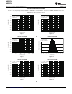
ADS1274 ADS1278 SBAS367F – JUNE 2007 – REVISED FEBRUARY 2011 www.ti.com TYPICAL CHARACTERISTICS At TA = +25°C, High-Speed mode, AVDD = +5V, DVDD = +1.8V, IOVDD = +3.3V, fCLK = 27MHz, VREFP = 2.5V, and VREFN = 0V, unless otherwise noted. OUTPUT SPECTRUM 0 OUTPUT SPECTRUM 0 High-Speed Mode fIN = 1kHz, -0.
ADS1274 ADS1278 SBAS367F – JUNE 2007 – REVISED FEBRUARY 2011 www.ti.com TYPICAL CHARACTERISTICS (continued) At TA = +25°C, High-Speed mode, AVDD = +5V, DVDD = +1.8V, IOVDD = +3.3V, fCLK = 27MHz, VREFP = 2.5V, and VREFN = 0V, unless otherwise noted.
ADS1274 ADS1278 SBAS367F – JUNE 2007 – REVISED FEBRUARY 2011 www.ti.com TYPICAL CHARACTERISTICS (continued) At TA = +25°C, High-Speed mode, AVDD = +5V, DVDD = +1.8V, IOVDD = +3.3V, fCLK = 27MHz, VREFP = 2.5V, and VREFN = 0V, unless otherwise noted. OUTPUT SPECTRUM 0 OUTPUT SPECTRUM 0 Low-Speed Mode fIN = 100Hz, -0.
ADS1274 ADS1278 SBAS367F – JUNE 2007 – REVISED FEBRUARY 2011 www.ti.com TYPICAL CHARACTERISTICS (continued) At TA = +25°C, High-Speed mode, AVDD = +5V, DVDD = +1.8V, IOVDD = +3.3V, fCLK = 27MHz, VREFP = 2.5V, and VREFN = 0V, unless otherwise noted. TOTAL HARMONIC DISTORTION vs FREQUENCY THD, THD+N (dB) -20 0 High-Resolution Mode VIN = -0.
ADS1274 ADS1278 SBAS367F – JUNE 2007 – REVISED FEBRUARY 2011 www.ti.com TYPICAL CHARACTERISTICS (continued) At TA = +25°C, High-Speed mode, AVDD = +5V, DVDD = +1.8V, IOVDD = +3.3V, fCLK = 27MHz, VREFP = 2.5V, and VREFN = 0V, unless otherwise noted. OFFSET DRIFT HISTOGRAM Multi-lot data based on 20°C intervals over the range -40°C to +105°C. 300 25 units based on 20°C intervals over the range -40°C to +105°C.
ADS1274 ADS1278 SBAS367F – JUNE 2007 – REVISED FEBRUARY 2011 www.ti.com TYPICAL CHARACTERISTICS (continued) At TA = +25°C, High-Speed mode, AVDD = +5V, DVDD = +1.8V, IOVDD = +3.3V, fCLK = 27MHz, VREFP = 2.5V, and VREFN = 0V, unless otherwise noted.
ADS1274 ADS1278 SBAS367F – JUNE 2007 – REVISED FEBRUARY 2011 www.ti.com TYPICAL CHARACTERISTICS (continued) At TA = +25°C, High-Speed mode, AVDD = +5V, DVDD = +1.8V, IOVDD = +3.3V, fCLK = 27MHz, VREFP = 2.5V, and VREFN = 0V, unless otherwise noted. 0.67 6.7 0.66 6.6 0.65 6.5 High-Speed and High-Resolution Modes 0.64 6.4 Low-Speed Mode 0.63 6.3 0.62 -40 0 20 40 60 Temperature (°C) 80 100 28.8 14.3 28.6 14.2 28.4 14.1 28.2 14.0 28.0 13.9 27.6 13.7 27.4 13.6 27.
ADS1274 ADS1278 SBAS367F – JUNE 2007 – REVISED FEBRUARY 2011 www.ti.com TYPICAL CHARACTERISTICS (continued) At TA = +25°C, High-Speed mode, AVDD = +5V, DVDD = +1.8V, IOVDD = +3.3V, fCLK = 27MHz, VREFP = 2.5V, and VREFN = 0V, unless otherwise noted. NOISE vs TEMPERATURE 14 14 12 12 12 10 10 Noise 8 8 6 6 Linearity 4 4 2 0 -0.
ADS1274 ADS1278 SBAS367F – JUNE 2007 – REVISED FEBRUARY 2011 www.ti.com TYPICAL CHARACTERISTICS (continued) At TA = +25°C, High-Speed mode, AVDD = +5V, DVDD = +1.8V, IOVDD = +3.3V, fCLK = 27MHz, VREFP = 2.5V, and VREFN = 0V, unless otherwise noted.
ADS1274 ADS1278 SBAS367F – JUNE 2007 – REVISED FEBRUARY 2011 www.ti.com TYPICAL CHARACTERISTICS (continued) At TA = +25°C, High-Speed mode, AVDD = +5V, DVDD = +1.8V, IOVDD = +3.3V, fCLK = 27MHz, VREFP = 2.5V, and VREFN = 0V, unless otherwise noted. ADS1278 IOVDD CURRENT vs TEMPERATURE ADS1278 POWER DISSIPATION vs TEMPERATURE 800 0.5 IOVDD Current (mA) 0.3 High-Speed Mode 0.2 Low-Power Mode 0.
ADS1274 ADS1278 SBAS367F – JUNE 2007 – REVISED FEBRUARY 2011 www.ti.com OVERVIEW High-Speed, High-Resolution, Low-Power, and Low-Speed. Table 2 summarizes the performance of each mode. The ADS1274 (quad) and ADS1278 (octal) are 24-bit, delta-sigma ADCs based on the single-channel ADS1271. They offer the combination of outstanding dc accuracy and superior ac performance. Figure 57 shows the block diagram.
ADS1274 ADS1278 SBAS367F – JUNE 2007 – REVISED FEBRUARY 2011 www.ti.com FUNCTIONAL DESCRIPTION The ADS1274/78 is a delta-sigma ADC consisting of four/eight independent converters that digitize four/eight input signals in parallel. The converter is composed of two main functional blocks to perform the ADC conversions: the modulator and the digital filter. The modulator samples the input signal together with sampling the reference voltage to produce a 1s density output stream.
ADS1274 ADS1278 SBAS367F – JUNE 2007 – REVISED FEBRUARY 2011 www.ti.com High-Speed, Low-Power, and Low-Speed Modes 0 -1 -2 Amplitude (dB) The digital filter configuration is the same in High-Speed, Low-Power, and Low-Speed modes with the oversampling ratio set to 64. Figure 58 shows the frequency response in High-Speed, Low-Power, and Low-Speed modes normalized to fDATA. Figure 59 shows the passband ripple. The transition from passband to stop band is shown in Figure 60.
ADS1274 ADS1278 SBAS367F – JUNE 2007 – REVISED FEBRUARY 2011 www.ti.com High-Resolution Mode 0 -1 -2 Amplitude (dB) The oversampling ratio is 128 in High-Resolution mode. Figure 62 shows the frequency response in High-Resolution mode normalized to fDATA. Figure 63 shows the passband ripple, and the transition from passband to stop band is shown in Figure 64. The overall frequency response repeats at multiples of the modulator frequency fMOD (128 × fDATA), as shown in Figure 65.
ADS1274 ADS1278 SBAS367F – JUNE 2007 – REVISED FEBRUARY 2011 www.ti.com Table 5. Ideal Output Code versus Input Signal PHASE RESPONSE The ADS1274/78 incorporates a multiple stage, linear phase digital filter. Linear phase filters exhibit constant delay time versus input frequency (constant group delay). This characteristic means the time delay from any instant of the input signal to the same instant of the output data is constant and is independent of input signal frequency.
ADS1274 ADS1278 SBAS367F – JUNE 2007 – REVISED FEBRUARY 2011 www.ti.com The ADS1274/78 uses switched-capacitor circuitry to measure the input voltage. Internal capacitors are charged by the inputs and then discharged. Figure 67 shows a conceptual diagram of these circuits. Switch S2 represents the net effect of the modulator circuitry in discharging the sampling capacitor; the actual implementation is different. The timing for switches S1 and S2 is shown in Figure 68.
ADS1274 ADS1278 SBAS367F – JUNE 2007 – REVISED FEBRUARY 2011 www.ti.com ESD diodes protect the reference inputs. To keep these diodes from turning on, make sure the voltages on the reference pins do not go below AGND by more than 0.4V, and likewise do not exceed AVDD by 0.4V. If these conditions are possible, external Schottky clamp diodes or series resistors may be required to limit the input current to safe values (see the Absolute Maximum Ratings table).
ADS1274 ADS1278 SBAS367F – JUNE 2007 – REVISED FEBRUARY 2011 www.ti.com MODE[1:0] Pins ADS1274/78 Mode Previous Mode New Mode tNDR-SPI SPI Protocol DRDY New Mode Valid Data Ready tNDR-FS Frame-Sync DOUT Protocol New Mode Valid Data on DOUT Figure 72. Mode Change Timing Table 10.
ADS1274 ADS1278 SBAS367F – JUNE 2007 – REVISED FEBRUARY 2011 www.ti.com tCSHD CLK tSCSU tSYN SYNC tNDR DRDY Figure 73. Synchronization Timing (SPI Protocol) Table 11. SPI Protocol SYMBOL DESCRIPTION MIN TYP MAX UNITS tCSHD CLK to SYNC hold time 10 ns tSCSU SYNC to CLK setup time 5 ns tSYN Synchronize pulse width 1 tNDR Time for new data to be ready CLK periods 129 Conversions (1/fDATA) tCSHD CLK tSCSU tSYN SYNC FSYNC tNDR Valid Data DOUT Figure 74.
ADS1274 ADS1278 SBAS367F – JUNE 2007 – REVISED FEBRUARY 2011 www.ti.com POWER-DOWN (PWDN) The channels of the ADS1274/78 can be independently powered down by use of the PWDN inputs. To enter the power-down mode, hold the respective PWDN pin low for at least two CLK cycles. To exit power-down, return the corresponding PWDN pin high. Note that when all channels are powered down, the ADS1274/78 enters a microwatt (μW) power state where all internal biasing is disabled.
ADS1274 ADS1278 SBAS367F – JUNE 2007 – REVISED FEBRUARY 2011 www.ti.com FORMAT[2:0] Data can be read from the ADS1274/78 with two interface protocols (SPI or Frame-Sync) and several options of data formats (TDM/Discrete and Fixed/Dynamic data positions). The FORMAT[2:0] inputs are used to select among the options. Table 14 lists the available options. See the DOUT Modes section for details of the DOUT Mode and Data Position. Table 14.
ADS1274 ADS1278 SBAS367F – JUNE 2007 – REVISED FEBRUARY 2011 www.ti.com FRAME-SYNC SERIAL INTERFACE DOUT Frame-Sync format is similar to the interface often used on audio ADCs. It operates in slave fashion—the user must supply framing signal FSYNC (similar to the left/right clock on stereo audio ADCs) and the serial clock SCLK (similar to the bit clock on audio ADCs). The data are output MSB first or left-justified on the rising edge of FSYNC.
ADS1274 ADS1278 SBAS367F – JUNE 2007 – REVISED FEBRUARY 2011 www.ti.com TDM Mode, Fixed-Position Data TDM Mode, Dynamic Position Data In this TDM data output mode, the data position of the channels remain fixed, regardless of whether the channels are powered down. If a channel is powered down, the data are forced to zero but occupy the same position within the data stream. Figure 78 shows the data stream with channel 1 and channel 3 powered down.
ADS1274 ADS1278 SBAS367F – JUNE 2007 – REVISED FEBRUARY 2011 www.ti.com SCLK 1 2 22 DOUT1 CH1 DOUT2 CH2 DOUT3 CH3 DOUT4 CH4 DOUT5 CH5 DOUT6 CH6 DOUT7 CH7 DOUT8 CH8 23 24 25 26 ADS1278 Only DRDY (SPI) FSYNC (Frame-Sync) Figure 80. Discrete Data Output Mode DAISY-CHAINING Multiple ADS1274/78s can be daisy-chained together to output data on a single pin. The DOUT1 data output pin of one device is connected to the DIN of the next device.
ADS1274 ADS1278 SBAS367F – JUNE 2007 – REVISED FEBRUARY 2011 SYNC CLK www.ti.com ADS1274/78 U2 SYNC ADS1274/78 U1 SYNC CLK CLK DIN SCLK DOUT1 DRDY DRDY Output from Device 1 DOUT1 DOUT from Devices 1 and 2 DIN SCLK SCLK NOTE: The number of chained devices is limited by the SCLK rate and device mode. Figure 81.
ADS1274 ADS1278 SBAS367F – JUNE 2007 – REVISED FEBRUARY 2011 www.ti.com POWER SUPPLIES MODULATOR OUTPUT The ADS1274/78 has three power supplies: AVDD, DVDD, and IOVDD. AVDD is the analog supply that powers the modulator, DVDD is the digital supply that powers the digital core, and IOVDD is the digital I/O power supply. The IOVDD and DVDD power supplies can be tied together if desired (+1.8V). To achieve rated performance, it is critical that the power supplies are bypassed with 0.
ADS1274 ADS1278 SBAS367F – JUNE 2007 – REVISED FEBRUARY 2011 www.ti.com In modulator output mode, the frequency of the modulator clock output (SCLK) depends on the mode selection of the ADS1274/78. Table 16 lists the modulator clock output frequency and DVDD current versus device mode. Figure 86 shows the timing relationship of the modulator clock and data outputs. The data output is a modulated 1s density data stream.
ADS1274 ADS1278 SBAS367F – JUNE 2007 – REVISED FEBRUARY 2011 www.ti.com APPLICATION INFORMATION To obtain the specified performance from the ADS1274/78, the following layout and component guidelines should be considered. 1. Power Supplies: The device requires three power supplies for operation: DVDD, IOVDD, and AVDD. The allowed range for DVDD is 1.65V to 1.95V; (for 32.768MHz < fCLK ≤ 37MHz: 2.0V to 2.2V) the range of IOVDD is 1.65V to 3.6V; AVDD is restricted to 4.75V to 5.25V.
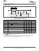
ADS1274 ADS1278 SBAS367F – JUNE 2007 – REVISED FEBRUARY 2011 www.ti.com THS4521 (1) ADS1274/ADS1278 IN1(+) AINP1 IN1(-) 2.2nF (3) +3.3V TMS320VC5509 IOVDD 10mF AINN1 CLK 50W DRDY/FSYNC ¼ ¼ DOUT1 DOUT2 DOUT3 AINP4/8 IN4/8(-) +5V 2.2nF + (3) AVDD (2) 10mF AINN4/8 +1.8V (6) DVDD (2) 10mF U1 0 Q CVDD (CORE) 50W +1.6V CLKR See Note (5) 200MHz DOUT4 SYNC PWDN1 I/O PWDN2 PWDN4 REF5025 + VREFP (2) 10mF 0.1mF VREFN CLKDIV +3.
ADS1274 ADS1278 SBAS367F – JUNE 2007 – REVISED FEBRUARY 2011 www.ti.com 1kW 1kW 1.5nF Buffered VCOM Output +5V (2) Buffered VCOM Output (1) AINP THS4521 49.9W 0.1mF AINN (3) 1.5nF 1kW 249W 5.6nF 49.9W VOCM VIN 1kW VIN +5V (1) 49.9W VOCM AINP THS4521 49.9W 0.1mF AINN (3) (2) 5.6nF 1kW 1kW (2) VO DIFF = 0.25 ´ VIN VO COMM = VREF (2) 249W (1) Bypass with 10μF and 0.1μF capacitors. (2) 2.7nF for Low-Power mode; 15nF for Low-Speed mode.
ADS1274 ADS1278 SBAS367F – JUNE 2007 – REVISED FEBRUARY 2011 www.ti.com PowerPAD THERMALLY-ENHANCED PACKAGING The PowerPAD concept is implemented in standard epoxy resin package material. The integrated circuit is attached to the leadframe die pad using thermally conductive epoxy. The package is molded so that the leadframe die pad is exposed at a surface of the package. This design provides an extremely low thermal resistance to the path between the IC junction and the exterior case.
ADS1274 ADS1278 SBAS367F – JUNE 2007 – REVISED FEBRUARY 2011 www.ti.com PowerPAD PCB Layout Considerations Figure 92 shows the recommended layer structure for thermal management when using a PowerPad package on a 4-layer PCB design. Note that the thermal pad is placed on both the top and bottom sides of the board. The ground plane is used as the heatsink, while the power plane is thermally isolated from the thermal vias.
ADS1274 ADS1278 SBAS367F – JUNE 2007 – REVISED FEBRUARY 2011 118mils (3mm) 40mils (1mm) 40mils (1mm) www.ti.com Package Outline Thermal Pad 40mils (1mm) 40mils (1mm) 118mils (3mm) 316mils (8mm) Thermal Via 13mils (0.33mm) 316mils (8mm) Figure 93.
ADS1274 ADS1278 SBAS367F – JUNE 2007 – REVISED FEBRUARY 2011 www.ti.com REVISION HISTORY NOTE: Page numbers for previous revisions may differ from page numbers in the current version. Changes from Revision E (September 2010) to Revision F • Page Deleted selective disclosure statement from document .......................................................................................................
PACKAGE OPTION ADDENDUM www.ti.
PACKAGE OPTION ADDENDUM www.ti.com 16-Jan-2012 Important Information and Disclaimer:The information provided on this page represents TI's knowledge and belief as of the date that it is provided. TI bases its knowledge and belief on information provided by third parties, and makes no representation or warranty as to the accuracy of such information. Efforts are underway to better integrate information from third parties.
PACKAGE MATERIALS INFORMATION www.ti.com 14-Jul-2012 TAPE AND REEL INFORMATION *All dimensions are nominal Device Package Package Pins Type Drawing ADS1274IPAPR HTQFP PAP 64 SPQ Reel Reel A0 Diameter Width (mm) (mm) W1 (mm) B0 (mm) K0 (mm) P1 (mm) W Pin1 (mm) Quadrant 1000 330.0 24.4 13.0 13.0 1.5 16.0 24.0 Q2 ADS1274IPAPT HTQFP PAP 64 250 330.0 24.4 13.0 13.0 1.5 16.0 24.0 Q2 ADS1278IPAPR HTQFP PAP 64 1000 330.0 24.4 13.0 13.0 1.5 16.0 24.
PACKAGE MATERIALS INFORMATION www.ti.com 14-Jul-2012 *All dimensions are nominal Device Package Type Package Drawing Pins SPQ Length (mm) Width (mm) Height (mm) ADS1274IPAPR HTQFP PAP 64 1000 367.0 367.0 45.0 ADS1274IPAPT HTQFP PAP 64 250 367.0 367.0 45.0 ADS1278IPAPR HTQFP PAP 64 1000 367.0 367.0 45.0 ADS1278IPAPT HTQFP PAP 64 250 367.0 367.0 45.
IMPORTANT NOTICE Texas Instruments Incorporated and its subsidiaries (TI) reserve the right to make corrections, enhancements, improvements and other changes to its semiconductor products and services per JESD46C and to discontinue any product or service per JESD48B. Buyers should obtain the latest relevant information before placing orders and should verify that such information is current and complete.