
Datasheet
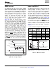

FORMAT0
DIN
ModulatorClockOutput
IOVDD
SCLK
FORMAT1
FORMAT2
ModulatorDataChannel2
DOUT2
ModulatorDataChannel1
DOUT1
ModulatorDataChannel4/8
(1)
DOUT4/8
(1)
DRDY
(SPIProtocol)
DOUT
(Frame-SyncProtocol)
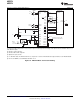
InternalReset
CLK
3Vnom
(1)
AVDD
1Vnom
(1)
IOVDD
1Vnom
(1)
DVDD
ValidData
2
18
f
CLK
129(max)
t
DATA
ADS1274
ADS1278
www.ti.com
SBAS367F –JUNE 2007– REVISED FEBRUARY 2011
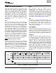
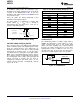
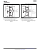
POWER SUPPLIES MODULATOR OUTPUT
The ADS1274/78 has three power supplies: AVDD, The ADS1274/78 incorporates a 6th-order, single-bit,
DVDD, and IOVDD. AVDD is the analog supply that chopper-stabilized modulator followed by a
powers the modulator, DVDD is the digital supply that multi-stage digital filter that yields the conversion
powers the digital core, and IOVDD is the digital I/O results. The data stream output of the modulator is
power supply. The IOVDD and DVDD power supplies available directly, bypassing the internal digital filter.
can be tied together if desired (+1.8V). To achieve The digital filter is disabled, reducing the DVDD
rated performance, it is critical that the power current, as shown in Table 16. In this mode, an
supplies are bypassed with 0.1μF and 10μF external digital filter implemented in an ASIC, FPGA,
capacitors placed as close as possible to the supply or similar device is required. To invoke the modulator
pins. A single 10μF ceramic capacitor may be output, tie FORMAT[2:0], as shown in Figure 85.
substituted in place of the two capacitors. DOUT[4:1]/[8:1] then becomes the modulator data
stream outputs for each channel and SCLK becomes
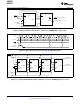
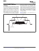
Figure 84 shows the start-up sequence of the
the modulator clock output. The DRDY/FSYNC pin
ADS1274/78. At power-on, bring up the DVDD supply
becomes an unused output and can be ignored. The
first, followed by IOVDD and then AVDD. Check the
normal operation of the Frame-Sync and SPI
power-supply sequence for proper order, including
interfaces is disabled, and the functionality of SCLK
the ramp rate of each supply. DVDD and IOVDD may
changes from an input to an output, as shown in
be sequenced at the same time (for example, if the
Figure 85.
supplies are tied together). Each supply has an
internal reset circuit whose outputs are summed
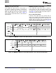
Table 16. Modulator Output Clock Frequencies
together to generate a global power-on reset. After
MODULATOR
the supplies have exceeded the reset thresholds, 2
18
CLOCK ADS1274 ADS1278
f
CLK
cycles are counted before the converter initiates
MODE OUTPUT DVDD DVDD
the conversion process. Following the CLK cycles,
[1:0] CLKDIV (SCLK) (mA) (mA)
the data for 129 conversions are suppressed by the
00 1 f
CLK
/4 4.5 8
ADS1274/78 to allow output of fully-settled data. In
01 1 f
CLK
/4 4.0 7
SPI protocol, DRDY is held high during this interval.
1 f
CLK
/8 2.5 4
In frame-sync protocol, DOUT is forced to zero. The
10
power supplies should be applied before any analog
0 f
CLK
/4 2.5 4
or digital pin is driven. For consistent performance,
1 f
CLK
/40 1.0 1
11
assert SYNC after device power-on when data first
0 f
CLK
/8 0.5 1
appear.
(1) The ADS1274 has four channels; the ADS1278 has eight
channels.
Figure 85. Modulator Output
(1) The power-supply reset thresholds are approximate.
Figure 84. Start-Up Sequence
© 2007–2011, Texas Instruments Incorporated Submit Documentation Feedback 35
Product Folder Link(s): ADS1274 ADS1278