
Datasheet


Contents
1 ADS1298ECG-FE/ADS1198ECG-FE Overview ......................................................................... 7
1.1 Important Disclaimer Information ...................................................................................... 7
1.2 Introduction ............................................................................................................... 8
1.3 Supported Features ..................................................................................................... 8
1.4 Features Not Supported in Current Version ......................................................................... 8
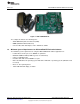
1.5 ADS1x98ECG-FE Hardware ........................................................................................... 8
1.6 Minimum System Requirements for ADS1x98ECG-FE Evaluation Software ................................... 9
2 Quick Start ....................................................................................................................... 10
2.1 Default Jumper/Switch Configuration ............................................................................... 10
2.2 ADS1x98ECG-FE Operation ......................................................................................... 11
3 Using the ADS1298ECG-FE Software ................................................................................... 12
3.1 Application User Menu ................................................................................................ 13
3.2 Top-Level Application Controls ....................................................................................... 13
3.3 About Tab ............................................................................................................... 14
3.4 ADC Register Tab ..................................................................................................... 15
3.5 Analysis Tab ............................................................................................................ 23
3.6 Save Tab ................................................................................................................ 31
4 ADS1x98ECG-FE Input Signals ........................................................................................... 33
4.1 Input Short Testing .................................................................................................... 33
4.2 Internal Test Signals Input ............................................................................................ 33
4.3 Temperature Sensor ................................................................................................... 34
4.4 Normal Electrode Input ................................................................................................ 35
4.5 MV
DD
Input, RLD Measurement, RLD Positive Electrode Driver, and RLD Negative Electrode Driver ..... 35
4.6 Lead Derivation ........................................................................................................ 36
4.7 Wilson Center Terminal (WCT) ...................................................................................... 36
4.8 Right Leg Drive ......................................................................................................... 36
4.9 PACE Detection ........................................................................................................ 37
5 ADS1298ECG-FE/ADS1198ECG-FE Hardware Details ............................................................. 39
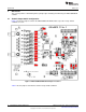
5.1 Jumper Description .................................................................................................... 40
5.2 Power Supply ........................................................................................................... 41
5.3 Clock ..................................................................................................................... 42
5.4 Reference ............................................................................................................... 42
5.5 Analog Output Signals ................................................................................................ 43
5.6 Digital Signals .......................................................................................................... 43
5.7 Analog Input Signals .................................................................................................. 43
Appendix A Schematics, BOM, Layout, and ECG Cable Details ....................................................... 45
A.1 ADS1x98ECG-FE Front-End Board Schematics ................................................................. 45
A.2 Bill of Materials ........................................................................................................ 46
A.3 Printed Circuit Board Layout ........................................................................................ 48
A.4 ECG Cable Details ................................................................................................... 50
Appendix B External Optional Hardware ...................................................................................... 51
2
Table of Contents SBAU171C–May 2010–Revised September 2012
Submit Documentation Feedback
Copyright © 2010–2012, Texas Instruments Incorporated