
Datasheet


www.ti.com
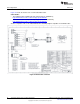
ADS1298ECG-FE/ADS1198ECG-FE Hardware Details
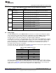
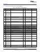
Table 5. ADS1x98ECG-FE Default Jumper/Switch Configuration (continued)
Jumper Function Settings
Open: Channel input not connected
CH5- connection
Installed: Channel input connected to WCT (requires JP16 to be installed)
JP29
Open: Channel input not connected
CH5+ connection
Installed: Channel input connected to ECG_V3
Open: Channel input not connected
CH4- connection
Installed: Channel input connected to WCT (requires JP16 to be installed)
JP30
Open: Channel input not connected
CH4+ connection
Installed: Channel input connected to ECG_V2
Open: Channel input not connected
CH3- connection
Installed: Channel input is connected to ECG_RA
JP31
Open: Channel input not connected
CH3+ connection
Installed: Channel input is connected to ECG_LL
Open: Channel input not connected
CH2- connection
Installed: Channel input is connected to ECG_RA
JP32
Open: Channel input not connected
CH2+ connection
Installed: Channel input is connected to ECG_ LA
Open: Channel input not connected
CH1- connection
Installed: Channel input connected to WCT (requires JP16 to be installed)
JP33
Open: Channel input not connected
CH1+ connection
Installed: Channel input connected to ECG_V6
5.2 Power Supply
The ADS1x98EVM mounts on the MMB0 EVM with connectors J2, J3 and J4. The main power supplies
(+5V, +3V and +1.8V) for the front-end board are supplied by the host board, MMB0, through connector
J4. All other power supplies needed for the front-end board are generated on board by power
management devices. The EVM is shipped in +3V unipolar supply configuration.
The ADS1298 can operate in a single supply with +3.0V to +5.0V analog supply (AVDD/AVSS) or bipolar
mode supply (±1.5V to ±2.5V). An additional digital supply of and +1.8V to +3.0V digital supply (DVDD) is
required for operation. The ADS1298EVM power consumption can be measured by removing the JP4
jumper and JP24 jumper to connect an ammeter. By shorting JP5, the ADS1298 can be placed in
powerdown mode for low power consumption.
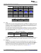
Test points TP5, TP6, TP7, TP8, TP9, TP10, and TP14 are provided to verify the power supplies voltages
are correct. The test points and voltages are shown in Table 6.
Table 6. Power-Supply Test Points
Test Point Voltage
TP7 +5.0V
TP9 +1.8V
TP10 +3.3V
TP5 +3.0V
TP13 +2.5V
TP6 –2.5V
TP8 GND
The front-end board must be properly configured in order to achieve the various power-supply schemes.
The default power-supply setting for the ADS1298ECG-FE is a bipolar analog supply of ±2.5V and DVDD
of either +3V or +1.8V. Table 7 shows the board and component configurations for each analog power-
supply scheme and Table 8 shows the board configurations for the digital supply.
41
SBAU171C–May 2010–Revised September 2012 ADS1298ECG-FE/ADS1198ECG-FE
Submit Documentation Feedback
Copyright © 2010–2012, Texas Instruments Incorporated