
Datasheet


ADS1298ECG-FE/ADS1198ECG-FE Hardware Details
www.ti.com
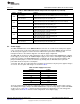
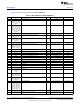
Table 7. Analog Supply Configurations (AVDD/AVSS)
Unipolar Analog Supply Bipolar Analog Supply
AVDD/AVSS 3V 5V ±1.5V ±2.5V
JP20 1-2 1-2 2-3 2-3
JP2 2-3 2-3 1-2 1-2
U7 TPS73230 TPS73250 Don't Care Don't Care
U9 Don't Care Don't Care TPS73201 TPS73201
U8 Don't Care Don't Care TPS72301 TPS72301
R52 Don't Care Don't Care 21kΩ 47.5kΩ
R53 Don't Care Don't Care 78.7kΩ 43kΩ
R56 Don't Care Don't Care 23.3kΩ 49.9kΩ
R57 Don't Care Don't Care 95.3kΩ 46.4kΩ
C87, C67, C62 Not Installed Not Installed Not Installed Not Installed
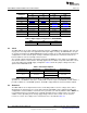
Table 8. Digital Supply Configurations (DVDD/DGND)
DVDD +3.0V +1.8V
JP24 1-2 2-3
5.3 Clock
The ADS1298 has an on-chip oscillator circuit that generates a 2.048MHz clock (nominal). This clock can
vary by ±5% over temperature. For applications that require higher accuracy, the ADS1298 also accepts
an external clock signal. The ADS1298ECG-FE provides an option to test both internal and external clock
configurations. For the external signal, circuitry is available to generate the external clock from an on-
board oscillator or from an externally connected source.
The external oscillator included on the EVM is powered from DVDD, the same supply as the ADS1298.
Care must be taken to ensure that the externally supplied clock oscillator can operate either with +1.8V or
+3.0V, depending on the DVDD supply configuration. Table 9 shows the jumper settings for the three
options for the ADS1298 clocks.
Table 9. CLK Jumper Options
ADS1298 Clock Internal Clock External OSC Clock External Clock
JP18 Not Installed 2-3 1-2
1-2 (Disable)
JP19 Don't Care Don't Care
2-3 (Enable)
A 2.048MHz oscillator installed on the EVM for +3V DVDD operation is FXO-HC735-2.048MHz. If
operation at +1.8V DVDD is desired, the oscillator will need to be replaced. SiT8002AC-34-18E-2.048 is a
possible oscillator for +1.8V DVDD operation. The EVM is shipped with the external oscillator enabled.
5.4 Reference
The ADS1298 has an on-chip internal reference circuit that provides reference voltages to the device.
Alternatively, the internal reference can be powered down and VREFP can be applied externally. This
configuration is achieved with the external reference generators (U3 and U4) and driver buffer. NOTE: U3,
U4, and driver buffer are not installed. The externally provided reference voltage can be set to either
4.096V or 2.5V, depending on the analog supply voltage. Measure TP3 to make sure the external
reference is correct. The settings for the external reference is described in Table 10.
42
ADS1298ECG-FE/ADS1198ECG-FE SBAU171C–May 2010–Revised September 2012
Submit Documentation Feedback
Copyright © 2010–2012, Texas Instruments Incorporated