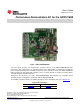
User's Guide SBAU200 – June 2012 Performance Demonstration Kit for the ADS131E08 Figure 1. ADS131E08EVM-PDK This user's guide describes the characteristics, operation, and use of the ADS131E08EVM-PDK. This performance demonstration kit is an evaluation module for the ADS131E08, an eight-channel, 24-bit, lowpower, integrated analog front-end (AFE) designed for power protection circuits. The ADS131E08EVMPDK is intended for prototyping and evaluation.
www.ti.com 1 2 3 4 5 6 Contents ADS131E08EVM OVERVIEW ............................................................................................ 4 SOFTWARE INSTALLATION ............................................................................................. 6 ADS131E08EVM Daughter-Card Hardware Overview ............................................................... 11 USING THE SOFTWARE ................................................................................................
www.ti.com 7 Serial Interface Pinout .................................................................................................... 14 8 Register Assignments: Channel-Specific Settings .................................................................... 17 9 GPIO: General-Purpose I/O Register ................................................................................... 20 10 ADS131E08 Bill of Materials SBAU200 – June 2012 Submit Documentation Feedback ..................................
ADS131E08EVM OVERVIEW www.ti.com 1 ADS131E08EVM OVERVIEW 1.1 Information about Cautions This document contains caution statements. The information in a caution statement is provided for your protection. Be sure to read each caution carefully. CAUTION This is an example of a caution statement. A caution statement describes a situation that could potentially damage your software or equipment. 1.
ADS131E08EVM OVERVIEW www.ti.com 1.4 ADS131E08EVM Hardware Figure 2 shows the hardware included in the ADS131E08EVM kit. Contact the factory at http://e2e.ti.com if any component is missing. Also, it is highly recommended that you check the TI website at http://www.ti.com to verify that you have the latest software. Figure 2.
SOFTWARE INSTALLATION www.ti.com 2 SOFTWARE INSTALLATION 2.1 Minimum Requirements Before installing the software that is intended for use with the EVM kit, please verify that your PCcompatible computer meets the following minimum requirements: • Pentium III® or Celeron® processor, 866 MHz or equivalent • Minimum 256 MB of RAM (512 MB or greater recommended) • USB 1.
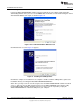
SOFTWARE INSTALLATION www.ti.com 2.2 Installing the Software CAUTION Do not connect the ADS131E08EVM hardware before installing the software on a suitable PC. Failure to observe this caution may cause Microsoft Windows to not recognize the ADS131E08EVM. Download the latest software from the TI website at www.ti.com/tool/ADS131E08EVM-PDK. To install the ADS131E08 software, unzip and run setup.exe. Figure 3 shows the initialization screen. Figure 3.
SOFTWARE INSTALLATION 2.3 2.3.1 www.ti.com Installing the ADS131E08EVM-PDK Hardware Drivers Installing the First USB Driver Apply power to the MMB0 using the supplied wall-mount power supply and connect the MMB0 to your PC through any available USB port. The Found New Hardware Wizard window appears, as shown in Figure 6. Note that this is the first of two USB drivers that are installed. Click Next to continue driver installation. Figure 6.
SOFTWARE INSTALLATION www.ti.com Navigate to C:\Program Files\ADS131E08EVM\USB Driver, as shown in Figure 8. Figure 8. New Hardware Wizard Screen 3 Click Next to find and install the driver. When the wizard is complete, the screen in Figure 9 appears. Figure 9.
SOFTWARE INSTALLATION 2.3.2 www.ti.com Installing the Second USB Driver Launch the ADS131E08EVM-PDK software from the program menu. The software loads and begins downloading firmware to the processor on the MMB0. After the firmware is loaded and running, the Found New Hardware Wizard starts again, as shown in Figure 10. Figure 10. Second New Hardware Wizard Screen Click Next and the screen in Figure 11 appears. Figure 11. Installing the USBStyx Driver Click Next to complete the installation.
ADS131E08EVM Daughter-Card Hardware Overview www.ti.com 3 ADS131E08EVM Daughter-Card Hardware Overview CAUTION Many of the components on the ADS131E08EVM are susceptible to damage by electrostatic discharge (ESD). Customers are advised to observe proper ESD handling procedures when unpacking and handling the EVM, including the use of a grounded wrist strap, bootstraps, or mats at an approved ESD workstation. An electrostatic smock and safety glasses should also be worn.
ADS131E08EVM Daughter-Card Hardware Overview www.ti.com The front-end board must be properly configured in order to achieve the various power-supply schemes. The default power-supply setting for the ADS131E08EVM is a bipolar analog supply of ±2.5 V, and there are onboard options to switch to a unipolar analog supply of +3 V. The digital supply (DVDD) is selectable to either +3.3 V or +1.8 V. Table 2 shows the board and component configurations for each analog powersupply scheme.
ADS131E08EVM Daughter-Card Hardware Overview www.ti.com 3.2 Clock The ADS131E08 has an on-chip oscillator circuit that generates a 2.048-MHz clock (nominal). This clock can vary by ±5% over temperature. For applications that require higher accuracy, the ADS131E08 can also accept an external clock signal. The ADS131E08 provides an option to test both internal and external clock configurations.
ADS131E08EVM Daughter-Card Hardware Overview 3.3.2 www.ti.com Accessing ADS131E08 Digital Supplies The ADS131E08 digital signals (including SPI signals, some GPIO signals, and some control signals) are available at connector J1. These signals are used to interface to the MMB0 board DSP. The pinout for this connector is shown in Table 7. Table 7. Serial Interface Pinout Signal 3.
USING THE SOFTWARE www.ti.com 4 USING THE SOFTWARE The software GUI contains a Save to File feature (located in the Save tab) that allows all data from any combination of channels, along with notes to describe the data, to be saved to a specified directory. This data can then be read back using a text editor. Saving the data in this format can be completed by clicking the Save to File button, as shown in Figure 12.
USING THE SOFTWARE 4.1 www.ti.com Software Overview This section provides a quick overview of the various features and functions of the ADS131E08EVM software package. There are four tabs across the left side of the GUI; from top to bottom, they are: • About: Provides information about the EVM and software version revisions.
USING THE SOFTWARE www.ti.com 4.3 Channel Control Registers The second section under the Channel Registers tab is the Channel Control Registers box. This panel allows the user to uniquely configure the front-end multiplexer (mux) for each channel. Additionally, at the top of the Channel Control Registers box is the option to globally set all channels to the same setting. Table 8 lists the register map.
USING THE SOFTWARE 4.4 www.ti.com Internal Test Signals Input and the Scope Display Tab Configuration Register 2 controls the signal amplitude and frequency of an internally-generated square wave test signal. The primary purpose of this test signal is to verify the functionality of the front-end mux, the programmable gain amplifier (PGA), and the ADC. The test signals may be viewed on the Analysis→Scope Display tab, as Figure 16 shows. Figure 16.
USING THE SOFTWARE www.ti.com 4.5 Temperature Sensor and the Scope Display Tab The internal temperature sensor on the ADS131E08 is shown in Figure 22. Temperature Sensor Monitor AVDD 1x 2x 8x 1x AVSS Figure 17.
USING THE SOFTWARE www.ti.com The number 0.1447 V (on the y-axis) can be calculated as a temperature using Equation 2: Temperature (°C) = 4.5.1 0.1447 - 0.145300 0.00049 + 25 = 23.78°C (2) MVDD Input and the Scope Tab The MVDD input option allows the measurement of the supply voltage VS = (AVDD + AVSS) / 2 for channels 1, 2, 5, 6, 7, and 8; however, the supply voltage for channel 3 is DVDD / 2. 4.
USING THE SOFTWARE www.ti.com 4.7 Fault Status Registers (FAULT_STATP and FAULT_STAIN) The Fault Status registers store the status of whether the positive and/or negative input on each channel has a fault. This is a convenient feature to help pinpoint if any of the inputs are out of range. The GUI for this feature is enabled by clicking in the upper right-hand corner of the EVM software on the Show/Poll Fault Status button, as shown in Figure 20. Figure 20.
USING THE SOFTWARE 4.8 www.ti.com Register Map The Register→Device Register tab is a helpful debug feature that allows the user to view the state of all the internal registers. This tab is shown in Figure 21. Figure 21.
ADS131E08 ANALYSIS TOOLS www.ti.com 5 ADS131E08 ANALYSIS TOOLS Under the Analysis tab in the ADS131E08 GUI software, there are three different analysis tools available that enable a detailed examination of the signals selected by the front-end mux: • Scope • Histogram • FFT 5.1 Scope Tool The Scope tool, available under the Analysis tab, is a very useful means of examining the data results in the time domain.
ADS131E08 ANALYSIS TOOLS 5.1.1 www.ti.com Scope Analysis Button The Scope Analysis button opens a pop-up window that displays the mean voltage, root mean square (RMS) voltage, and peak-to-peak voltage for noise analysis. Figure 23 shows an example of this window. Figure 23. Scope Analysis Tab (Noise Levels for Each Channel Shown) 5.1.2 Waveform Examination Tool The waveform examination tool allows the user to either zoom in on all channels simultaneously, or on just a single channel.
ADS131E08 ANALYSIS TOOLS www.ti.com 5.2 Histogram Tool The Histogram subtab displays the data in a histogram format for the eight channels. The data set is arranged in the total number of histogram bins set within the tab following acquisition. The screen shot shown in Figure 25 illustrates the histogram output for an input shorted signal. The same signal-zoom analysis shown in the previous section may be used on the histogram plots for a more detailed examination of the amplitude bins.
ADS131E08 ANALYSIS TOOLS 5.3 www.ti.com FFT Tool The FFT subtab displays the data in the frequency domain by performing an FFT on the eight channels. Details of the FFT, including SNR, THD, and more, can be viewed using the FFT Analysis button located at the bottom of the display. Figure 27 shows the FFT display. Figure 27. Analysis→FFT Graph of Normal Electrode Configuration 5.3.1 Coherent Frequency Calculator The red box labeled 1 in Figure 27 shows the Coherent Frequency Calculator.
ADS131E08 ANALYSIS TOOLS www.ti.com 5.3.2 AC Analysis Parameters The AC Analysis Parameters portion of the FFT tool (red box 2 in Figure 27) is used to dictate the number of harmonics, dc leakage bins, harmonic leakage bins, and fundamental leakage bins that are used in the creation of various histograms. Press the Windowing button, shown in in Figure 28, to evaluate the FFT graph under a variety of different windowing options.
ADS131E08 ANALYSIS TOOLS 5.3.4 www.ti.com User-Defined Dynamic Range This portion of the FFT tool (red box 4, Figure 27) is used to examine the SNR of a specific channel within a given frequency band defined by the Low Frequency and High Frequency fields. The SNR displayed in this window also appears under the Dynamic Range heading, as shown in Figure 30. Figure 30. Changing the User-Defined Dynamic Range for Channel 1 5.3.
www.ti.com 6 BILL OF MATERIALS (BOM), LAYOUT, AND SCHEMATIC BILL OF MATERIALS (BOM), LAYOUT, AND SCHEMATIC This section contains the complete BOM, printed circuit board (PCB) layouts, and schematic diagrams for the ADS131E08. NOTE: Board layouts are not to scale. These figures are intended to show how the board is laid out; they are not intended to be used for manufacturing ADS131E08 PCBs.
BILL OF MATERIALS (BOM), LAYOUT, AND SCHEMATIC 6.1 www.ti.com Bill of Materials Table 10 lists the bill of materials for the ADS131E08. Table 10.
BILL OF MATERIALS (BOM), LAYOUT, AND SCHEMATIC www.ti.com Table 10. ADS131E08 Bill of Materials (continued) Item Qty Ref Des 25 0 R5, R6, R8, R9, R11, R12, R14, R15, R17, R18, R20, R21, R23, R24, R26, R27, R29, R30, R32, R33, R35, R36, R38, R39, R41, R42, R44, R45, R47, R48, R50, R51, R52, R53, R54, R55, R56, R57, R58, R64, R65, R66 Description Manufacturer Part Number 26 1 R59 RES 49.9K OHM 1/10W 1% 0603 SMD Yageo RC0603FR-0749K9L 27 1 R60 RES 46.
BILL OF MATERIALS (BOM), LAYOUT, AND SCHEMATIC 6.2 www.ti.com PCB Layout The ADS131E08 PCB layout is appended to this document. 6.3 Front-End Board Schematic The ADS131E08 schematic is appended to this document.
Top Assembly Top Layer
Internal Layer 1 Internal Layer 2
Bottom Layer Bottom Assembly
1 2 AVDD AVSS 3 4 AVDD AVDD D1 NI IN1N C64 470pF D AVSS R5 NI R4 10k IN2N 10k C22 470pF AVSS AVDD CH1 R8 NI R7 10k C65 470pF R17 NI C20 470pF PG2 R18 NI D NI AVSS AVSS J7 AVDD AVDD AVSS AVDD D7 NI PG2 R14 NI R13 R9 NI IN2P 10k C23 470pF AVSS AVSS AVDD 2 1 CH2 IN1P AVDD IN3N 10k AVSS 2 1 2 1 D2 NI R16 PG2 R12 J6 AVDD D4 NI AVSS AVSS AVSS R11 NI R10 R6 NI AVDD AVDD D6 NI PG2 AVSS J5 6 5 D10 NI CH3 R19 IN3P 10k PG2 R20 NI C70 470pF R1
1 2 3 4 6 5 D D TP15 TP14 TP16 R1 GPIO1 GPIO2 GPIO3 GPIO4 2 4 6 8 10 1 3 5 7 9 C3 0 J4 1uF C13 /PWDN DAISY_IN AVSS VCAP3 AVDD 0.1uF NI AGND AVSS 63 62 61 60 21 19 58 57 20 23 56 59 22 55 54 53 C68 1uF AVDD U1 ADS13xE08 C6 C16 C7 C19 C8 C15 1uF 0.1uF NI NI NI NI AVSS AVSS AGND AVDD AVDD DVDD C4 C14 C17 C18 C12 C5 1uF 0.1uF 1uF 0.1uF 0.
1 2 3 4 6 5 D D External Reference 2 3 C26 4 NI N/C VIN R55 C32 7 C27 TEMP GND NI 6 OUT NI NI AVDD 5 TRIM C35 AVSS C33 NI 7 1 U2 NI N/C AVDD N/C 8 External Reference Drivers NI 8 AGND 1 2 3 C28 4 NI N/C VIN U3 NI JP12 N/C AVDD N/C C R54 NI NI OUT 6 C29 TEMP GND R52 3 R56 JP2 NI NI VREFP NI C30 NI C31 NI C34 NI AGND NI TRIM 6 NI C R53 NI U4 4 7 2 8 AVSS 5 C36 AVSS AVSS NI AVSS NOT INSTALLED B B ti A A 12500 TI Boulevard.
1 2 3 4 6 5 C40 D D 3 5 1uF 10uF C39 10uF 1uF IN OUT 1 C42 1uF 10uF TPS60403 AGND VCC_-5v 470uH C41 C43 10uF AGND AGND 4 AGND C38 CFLY- 2 470uH L2 GND C37 TP4 U5 L1 CFLY+ VCC_5v AGND TP5 U6 1 IN OUT L3 5 C44 C 1uF 3 R57 NI EN C45 C46 2.2uF 10uF 470uH +3.0V JP1 C47 AVDD C 10uF AGND AGND 2 AGND GND NR/FB AGND 4 C49 TPS73230 R58 NI C48 0.1uF NI AGND AGND TP13 U8 1 IN OUT L5 5 C50 1uF 3 EN C52 2.2uF 10uF +2.
1 2 3 4 6 5 D D DVDD DVDD C63 100uF R63 10K C62 J3 J2 1 3 5 7 9 11 13 15 17 19 C JP10 J1 2 4 6 8 10 12 14 16 18 20 JP8 SPI_CLK SPI_CS SPI_IN SPI_OUT SPI_DRDY EXT_CLK 1 3 5 7 9 11 13 15 17 19 CLKSEL TP7 2 4 6 8 10 12 14 16 18 20 VCC_5v JP3 GPIO1 /RESET GPIO2 VCC_3.3V C75 C60 C61 100uF 0.1uF SPI_START JP9 SCL AGND SDA 8 6 5 7 VCC SCL SDA WP AGND 0.1uF 1 3 5 7 9 TP9 VCC_1.8V JP11 VCC_3.3V TP10 TP8 C 0.1uF VCC_3.
Evaluation Board/Kit Important Notice Texas Instruments (TI) provides the enclosed product(s) under the following conditions: This evaluation board/kit is intended for use for ENGINEERING DEVELOPMENT, DEMONSTRATION, OR EVALUATION PURPOSES ONLY and is not considered by TI to be a finished end-product fit for general consumer use. Persons handling the product(s) must have electronics training and observe good engineering practice standards.
EVALUATION BOARD/KIT/MODULE (EVM) ADDITIONAL TERMS Texas Instruments (TI) provides the enclosed Evaluation Board/Kit/Module (EVM) under the following conditions: The user assumes all responsibility and liability for proper and safe handling of the goods. Further, the user indemnifies TI from all claims arising from the handling or use of the goods.
FCC Interference Statement for Class B EVM devices This equipment has been tested and found to comply with the limits for a Class B digital device, pursuant to part 15 of the FCC Rules. These limits are designed to provide reasonable protection against harmful interference in a residential installation. This equipment generates, uses and can radiate radio frequency energy and, if not installed and used in accordance with the instructions, may cause harmful interference to radio communications.
【Important Notice for Users of this Product in Japan】 】 This development kit is NOT certified as Confirming to Technical Regulations of Radio Law of Japan If you use this product in Japan, you are required by Radio Law of Japan to follow the instructions below with respect to this product: 1. 2. 3. Use this product in a shielded room or any other test facility as defined in the notification #173 issued by Ministry of Internal Affairs and Communications on March 28, 2006, based on Sub-section 1.
EVALUATION BOARD/KIT/MODULE (EVM) WARNINGS, RESTRICTIONS AND DISCLAIMERS For Feasibility Evaluation Only, in Laboratory/Development Environments. Unless otherwise indicated, this EVM is not a finished electrical equipment and not intended for consumer use.
IMPORTANT NOTICE Texas Instruments Incorporated and its subsidiaries (TI) reserve the right to make corrections, enhancements, improvements and other changes to its semiconductor products and services per JESD46, latest issue, and to discontinue any product or service per JESD48, latest issue. Buyers should obtain the latest relevant information before placing orders and should verify that such information is current and complete.