ADS5423/24/33 and ADS5411 EVM User Guide User's Guide February 2006 SLWU020B
SLWU020B – February 2005 – Revised February 2006 Submit Documentation Feedback
Contents 1 Overview ................................................................................................................... 5 1.1 Purpose .............................................................................................................. 5 1.2 EVM Basic Functions............................................................................................... 5 1.3 Power Requirements ...............................................................................................
List of Figures 4-1 4-2 4-3 4-4 4-5 4-6 Top Layer.................................................................................................................... Layer 2, Ground Plane .................................................................................................... Layer 3, Power Plane #1 .................................................................................................. Layer 4, Power Plane #2 ...........................................................................
Chapter 1 SLWU020B – February 2005 – Revised February 2006 Overview This User’s Guide document gives a general overview of the ADS5423/24/33 and ADS5411 evaluation module (EVM) and provides a general description of the features and functions to be considered while using this module. 1.1 Purpose The EVM provides a platform for evaluating the ADS5423/24/33 14-bit analog-to-digital converter (ADC) under various signals, references, and supply conditions.
www.ti.com EVM Operational Procedure Table 1-1. Three Pin Jumper List Table JUMPER FUNCTION LOCATION: PINS 1–2 LOCATION: PINS 2–3 DEFAULT Source provided from Diff Amp 1–2 SJP3 Provides AIN+ source to ADC device Source provided from T2 SJP4 Provides AIN– source to ADC device Source provided from Diff Amp Source provided from T2 2-3 2. Connect supplies to the EVM as follows: +5 V (4.75 V–5.25 V) ADC analog supply to J3 and return to J2. +3.3 V (3 V–3.
Chapter 2 SLWU020B – February 2005 – Revised February 2006 Circuit Description 2.1 Schematic Diagram The schematic diagram for the EVM is attached at the end of this document. 2.2 Circuit Function The following paragraphs describe the function of EVM circuits. See the relevant data sheet for the device operating characteristics. 2.2.1 Analog Inputs The EVM can be configured to provide the ADC with either transformer-coupled or differential amplifier inputs from a single-ended source.
www.ti.com Circuit Function Table 2-1.
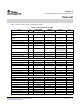
Chapter 3 SLWU020B – February 2005 – Revised February 2006 Parts List Table 3-1 lists the parts used in constructing the EVM Table 3-1. Bill of Materials for EVM VALUE QTY PART NUMBER VENDOR REF DES NOT INSTALLED 0.1 µF, 25 V, +80/–20% Capacitor 4 ECJ-0EF1E104Z Panasonic C1, C2, C3, C4 0.
www.ti.com Table 3-1.
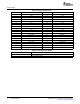
Chapter 4 SLWU020B – February 2005 – Revised February 2006 Physical Description This chapter describes the physical characteristics and PCB layout of the EVM and lists the components used on the module. 4.1 PCB Layout The EVM is constructed on a 6-layer, 4.77-inch × 3.4-inch, 0.062-inch thick PCB using FR-4 material. The individual layers are shown in Figure 4-1 through Figure 4-6. Figure 4-1.
www.ti.com PCB Layout Figure 4-2.
www.ti.com PCB Layout Figure 4-3.
www.ti.com PCB Layout Figure 4-4.
www.ti.com PCB Layout Figure 4-5.
www.ti.com PCB Layout Figure 4-6.
www.ti.com Schematics 4.
1 2 3 4 5 6 D D +VCC J10 SMA_PCB_MT_MOD 5 4 3 2 R4 49.9 CLK+ 4 CLK+ (Sh 2) R6 24.9 U3 2 NC C2 1 499 R10 49.9 .1uF 5 499 3 3 C1 5 4 3 2 1 C 1 T3 ADT 4-1WT R14 7 J5 SMA_PCB_MT_MOD R17 CLK- 6 8 CLK- (Sh 2) .1uF 2 C40 THS4503 C +VCC 5 + C26 VCM VOUT- 20pF VOCM R23 VOUT+ .1uF 1 4 - 49.9 -VCC -VCC 4 6 -VCC U4 2 6 R15 R27 499 499 24.9 +VCC (2-1) SJP3 J11 SMA_PCB_MT_MOD 1 1 5 4 3 2 T2 ADT 1-1WT 6 R2 R9 5 49.9 R11 24.9 AIN+ 36.
9 10 (Sh 1) AIN+ (Sh 1) AIN- AIN+ 11 AIN- 12 13 (Sh 3) (Sh 3) D OVR (Sh 3) 6 OVR D0 D0 (Sh 3) D1 D1 (Sh 3) D2 D2 D3 D3 (Sh 3) (Sh 3) D4 40 D4 D5 41 D5 (Sh 3) (Sh 3) D6 44 D6 (Sh 3) D7 45 D7 (Sh 3) D8 46 D8 (Sh 3) D9 47 D9 (Sh 3) D10 48 D10 (Sh 3) D11 49 D11 D12 50 D12 D13 D13 DRY 52 D4 D5 42 DVSS 43 DVDD D6 D7 D8 D9 D10 D11 D12 -ENC DVSS LVSS DVDD LVDD OVR CVDD DNC CVSS AVDD +AIN ADVSS -AIN ADVDD AVSS AVDD 8 DMID ADS5424 A
1 2 D 3 4 5 6 D DRVDD C15 + C16 C17 C18 C19 C20 C21 C22 C23 .1uF .1uF .1uF .
1 2 3 4 5 6 +3.3VA-PS DRVDD J4 L5 1 D 2 DRVDD D + J6 C13 C14 33uF .1uF GND L6 1 2 (Note 1) 3.3V_DVDD J1 L1 1 2 DVDD + C5 C6 C27 C28 C29 C47 C48 C49 .1uF .01uF .01uF .01uF 200pF 200pF 200pF C C 33uF J2 GND C8 C30 C31 C32 C33 C34 C35 C41 C42 C43 C44 C45 C46 .1uF .01uF .01uF .01uF .01uF .01uF .01uF 200pF 200pF 200pF 200pF 200pF 200pF C7 + J3 L2 1 33uF 5V_AVDD 2 AVDD J8 1 L3 +VCC 2 +VCC C9 C11 C36 C37 33uF .1uF .
www.ti.com Schematics EVALUATION BOARD/KIT IMPORTANT NOTICE Texas Instruments (TI) provides the enclosed product(s) under the following conditions: This evaluation board/kit is intended for use for ENGINEERING DEVELOPMENT, DEMONSTRATION, OR EVALUATION PURPOSES ONLY and is not considered by TI to be a finished end-product fit for general consumer use. Persons handling the product(s) must have electronics training and observe good engineering practice standards.
www.ti.com Schematics FCC Warning This evaluation board/kit is intended for use for ENGINEERING DEVELOPMENT, DEMONSTRATION, OR EVALUATION PURPOSES ONLY and is not considered by TI to be a finished end-product fit for general consumer use. It generates, uses, and can radiate radio frequency energy and has not been tested for compliance with the limits of computing devices pursuant to part 15 of FCC rules, which are designed to provide reasonable protection against radio frequency interference.
IMPORTANT NOTICE Texas Instruments Incorporated and its subsidiaries (TI) reserve the right to make corrections, modifications, enhancements, improvements, and other changes to its products and services at any time and to discontinue any product or service without notice. Customers should obtain the latest relevant information before placing orders and should verify that such information is current and complete.