
User's Guide Power Supply ADS5525, 27, 45, 46, 47,


www.ti.com
3 Circuit Description
3.1 Schematic Diagram
3.2 Circuit Function
3.2.1 Configuration Options
3.2.2 Power
Circuit Description
The schematic diagram for the EVM is in Section 5.3 of this document.
The following paragraphs describe the function of individual circuits. See the data sheet for complete
device operating characteristics.
The EVM provides a DIP switch, SW1, to control many of the modes of operation when the EVM is
configured for parallel-mode operation. Table 1 describes the functionality of the DIP switches.
Note: When the device is configured for serial-mode operation (SW1, switch 8), the DIP settings
on SW1, switch 1 through SW1, switch 7 are ignored.
Table 1. DIP Switch SW1
SW1 SWITCH
OFF ON DESCRIPTION
NUMBER
1 2s complement Offset binary Determines device output format
2 LVDS CMOS Determines device output mode
3 Reserved Reserved Reserved
4 Internal reference External reference When set to External Reference, ADC uses common-mode
voltage on TP1.
5 Edge = 1 Edge = 2 Allows for output edge programmability
6 Edge = 3 Edge = 4 Allows for output edge programmability
7 Normal Power down Allows for power down
8 Serial Parallel Determines mode for register interface
By switching SW1, switch 8 to OFF, the ADC operates in serial mode, using its programmed register
contents. A complete register map can be found in the device datasheet. Three pins on header J6 have
been reserved for programming the device while it operates in serial mode. To program the device
registers using header J6, place SCLK on pin 21, SDATA on pin 23, and SEN on pin 25. A pattern
generator can be used to generate the patterns needed for programming. Alternatively, TI provides an
optional USB daughtercard that plugs into the expansion slot of the EVM. The USB daughtercard allows
ADC register control via a software package loaded onto the PC.
Power is supplied to the EVM via banana jack sockets. The EVM offers the capability to supply analog
and digital 3.3 V independently to the ADC. Table 2 offers a snapshot of the power-supply options. All
supply connections are required for default operation, except J12, J10, J13, and J20.
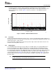
The EVM provides local decoupling for the ADC; however, the ADC features internal decoupling, and in
many cases minimal external decoupling can be used without loss in performance. Users are encouraged
to experiment to find the optimal amount of external decoupling required for their application. Figure 1
shows the ADS5547 LVDS-mode performance with all of the decoupling capacitors installed and the
performance with C4, C5, C6, C7, C8, C9, and C10 removed. By default, the EVM comes with all of the
decoupling capacitors installed.
SLWU028B – January 2006 – Revised November 2006 7
Submit Documentation Feedback