ADS62PXXEVM User's Guide Literature Number: SLAU237A May 2008 – Revised April 2009
SLAU237A – May 2008 – Revised April 2009 Submit Documentation Feedback
Contents 1 Overview ............................................................................................................................. 6 .............................................................................. 6 Circuit Description ............................................................................................................... 8 2.1 Schematic Diagram ....................................................................................................... 8 2.
www.ti.com List of Figures 1 2 3 4 5 6 7 8 9 10 11 12 13 14 15 16 17 18 19 20 21 22 23 24 4 ADS62PXX Jumpers ........................................................................................................ 8 ADS62PXX Surface Jumpers .............................................................................................. 9 ADS62PXXEVM Power Distribution ..................................................................................... 10 CDCE72010 EEPROM Configuration Block Diagram ......
www.ti.com List of Tables 1 2 3 4 5 6 7 8 9 Jumper List ................................................................................................................... 7 EVM Power Supply Jumper Description ................................................................................ 11 EVM Power Supply Options .............................................................................................. 11 Analog Input Jumper description .............................................................
User's Guide SLAU237A – May 2008 – Revised April 2009 ADS62PXXEVM 1 Overview This user’s guide gives a general overview of the evaluation module (EVM) and provides a general description of the features and functions to be considered while using this module. This manual is applicable to the ADS62P42/43/44/45/48/49, ADS62P22/23/24/25/28/29 and ADS62C15/17 analog to digital converters (ADC), which will be collectively referred to as ADS62PXX.
Overview www.ti.com Table 1.
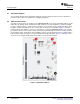
Circuit Description 2 Circuit Description 2.1 Schematic Diagram www.ti.com The schematic diagram for the this EVM is attached at the end of this document. See the schematic or relevant section of this user's guide before changing any jumpers. 2.2 ADC Circuit Function Selection of various modes of operation of the ADS62PXX EVM is most often controlled by jumpers on the EVM, either by placing shunts on 0.025-inch square jumper posts or by installation of surface mount 0Ω resistors.
Circuit Description www.ti.com Figure 2. ADS62PXX Surface Jumpers 2.2.1 ADC Operational Mode By default, the ADC is configured to operate in parallel-mode operation, since jumper (JP11) asserts a 3.3V state to the ADC reset pin. Consequently, the SW1 reset pushbutton must be pressed only when the device is configured in serial operation mode. Since the ADC is in parallel operation mode, voltages are used to set the ADC configuration modes.
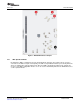
Circuit Description www.ti.com Figure 3. ADS62PXXEVM Power Distribution 2.2.2 EVM Power Connections Power is supplied to the EVM through banana jacks. From this input power, several different ways of delivering power to the ADC and other EVM functions are available. Figure 3 shows a simplified representation of the power options available for the ADS62PXXEVM. The default option is to provide 5V to the red banana jack J10, and from there, the EVM generates 3.
Circuit Description www.ti.com Table 2. EVM Power Supply Jumper Description EVM Banana Jack Description Jumper J10 Input Setting 6V to 36V power supply default-apply just 5V JP16 TPS79501 INPUT SELECT 1-2 → Connects 5.3V to input of TPS79501 2-3 → TPS79501 Input connected to J10 JP19 5V_AUX 2-3 → TPS79501 output as 5V_AUX rails 1-2 → 5V_AUX rail connected to J10 JP17 TPS5420 INPUT SELECT Shunt → J10 connected to TPS5420D Table 3. EVM Power Supply Options 2.2.2.
Circuit Description 2.2.2.3 www.ti.com Power Supply Option 3 Option 3 is used to evaluate ADC performance using an isolated AVDD and DVDD power supply for current-consumption measurements. This option must be used with caution, because reversing the power supply or connecting to the wrong connector can damage the EVM. One common use of this option is to measure the separate current consumption of the relative supplies under particular operating conditions.
Circuit Description www.ti.com Table 5. EVM Analog Input Options EVM Option 1 2 2.2.3.
Circuit Description www.ti.com Alternatively, the clock may be supplied by an onboard VCXO and CDCE72010 clock buffer. The CDCE72010 Clock Buffer has been factory programmed to output a clock to the ADC that is 1/4 the rate of the on-board VCXO. While using this clock option, a separate 20MHz reference clock must be supplied to the CDCE72010 by way of the Clock Input SMA connector J19 (Surface jumper SJP4 should be shorted to position 2-3 for this case).
Circuit Description www.ti.com Table 7. EVM Clock Input Options EVM Option 2.2.4.
Circuit Description www.ti.com Figure 4. CDCE72010 EEPROM Configuration Block Diagram 2.2.4.3 Clock Option 3 Option 3 is used for a differential LVPECL clock. This configuration eliminates the need for a crystal filter. It uses the same EEPROM configuration as Option 2, but in this case, the ADC clock pins are connected to Y1N and Y1P. The jumper setting uses the clock output Y1P and Y1N from CDCE72010, to clock ADC. This configuration is not recommended for SNR critical applications.
TI ADC SPI Control Interface www.ti.com 3 TI ADC SPI Control Interface This section describes the software features of the EVM kit. The TI ADC SPI control software provides full control of the SPI interface, allowing users to write to any of the ADC registers found in the data sheet. For most ADS62PXX performance evaluations, users do not need to use the TI SPI control software.
TI ADC SPI Control Interface www.ti.com Figure 6. Window Logo Testing Figure 7. Hardware Device Manager 3.2 Setting Up the EVM for ADC SPI Control Users who wish to use the ADC SPI interface must supply 5 VDC to P5, which provides power to the USB circuit. By default, the EVM comes with the ADC configured in parallel mode. In order to use the SPI interface to control the ADC modes of operation, users must move several jumpers.
TI ADC SPI Control Interface www.ti.com 3.3 Using the TI ADC SPI Interface Software Once the software is installed and the USB cable is connected, three primary modes of operating the software are available: SPI Register Writes, SPI Register Write Using a Script File, and ADS62PXX Frequently Used Registers. Note: Before beginning an ADC evaluation, users are required to reset the ADC. This can easily be done by pressing the ADS62PXX Reset button found on the ADS62PXX tab.
TI ADC SPI Control Interface 3.3.1 www.ti.com SPI Register Writes The most basic mode of operation allows full control of writing to individual register addresses. From the tabs at the top of the interface screen (Figure 8), select the ADS62PXX ADC. Next, type the Address Bytes(s) in hexadecimal (hex) and Data Byte(s) in hex, which can be found in the device data sheet. When you are ready to send this command to the ADC, either press "Enter" on your keyboard or press the Send Data button.
Connecting to FPGA Platforms www.ti.com 4 Connecting to FPGA Platforms The ADS62PXX EVM provides several connection options to use the EVM with various FPGA development platforms and FPGA-based capture boards. The ADC features two output options, a DDR LVDS which interfaces with a TSW1200 capture card, and a CMOS output which interfaces with a TSW1100 capture card. 4.1 TSW1200 Capture Board The TSW1200 board can be used to analyze the performance of the EVM.
Connecting to FPGA Platforms 4.1.1 www.ti.com Quick-Test Results The user can make the jumper setting as mentioned in Table 1. In this configuration, the EVM uses an external clock source from J19 and a direct input signal J6 (Channel A) or J3 (Channel B) to the ADC. This setup uses Power Option 2 (Table 3), Analog Input Option 1 (Table 5), and Clock Option 1 (Table 7), which is the default on the EVM. Figure 10 shows the ADC performance capture using TSW1200 with the input signal of a 57.
www.ti.com 4.1.2 Connecting to FPGA Platforms Test Result With Onboard VCXO and Clock Through Crystal Filter This test uses the VCXO of frequency 983.04 MHz. This setup uses the Power Option 2 (Table 3), Analog Input Option 1 (Table 5), and Clock Option 2 (Table 7). For this test, the CDCE72010 crystal filter path was chosen to provide the clock to the ADC. The CDCE72010 provides a single-ended clock through output Y0 (Table 7), which is passed through a crystal filter of center frequency 245.76 MHz.
Connecting to FPGA Platforms 4.1.3 www.ti.com Test Result With Onboard VCXO and Differential LVPECL Clock For the same setup as explained in the previous section, when Clock Option 3 (Table 7) was used, the FFT was captured as shown in Figure 12. The test results with Clock Option 2 are better than with Clock Option 3. That is why Option 2 (clock with crystal filter) is recommended over the differential LVPECL output. Figure 12.
www.ti.com 5 ADC Evaluation ADC Evaluation This section describes how to set up a typical ADC evaluation system that is similar to what TI uses to perform testing for data-sheet generation. Consequently, the information in this section is generic in nature and is applicable to all high-speed, high-resolution ADC evaluations. This section covers signal tone analysis, which yields ADC data sheet figures of merit such as signal-to-noise ratio (SNR) and spurious free dynamic range (SFDR). 5.
ADC Evaluation 5.2 www.ti.com Coherent Input Frequency Selection Typical ADC analysis requires users to collect the resulting time-domain data and perform a Fourier transform to analyze the data in the frequency domain. A stipulation of the Fourier transform is that the signal must be continuous-time; however, this is impractical when looking at a finite set of ADC samples, usually collected from a logic analyzer.
Physical Description www.ti.com 6 Physical Description This section describes the physical characteristics and PCB layout of the EVM. 6.1 PCB Layout The EVM is constructed on a four-layer, 0.062-inch thick PCB using FR-4 material. The individual layers are shown in Figure 13 through Figure 18. The layout features a split ground plane; however, similar performance can be obtained with careful layout using a common ground plane. Figure 13.
Physical Description www.ti.com Figure 14. Component Side Figure 15.
Physical Description www.ti.com Figure 16. Layer 2 Figure 17.
Physical Description www.ti.com Figure 18.
Physical Description www.ti.com 6.2 Bill of Materials Table 9. Bill of Materials Qty Reference Value Footprint MFR Part Number DNI = Do Not Install 4 C1,C6,C43,C64 1µF 603 Panasonic ECJ-1VB1A105K 15 C2, C8, C19–C23, C52–C59 0.1µF 603 Panasonic ECJ-1VB1C104K 4 C3, C5, C7, C10 22µF smd_cap_1210_pol Kemet T491A226M010AT 2 C4, C9 10µF smd_cap_1210_pol Kemet B45197A3106K209 23 C11–C18, C33,C35–C37, C40,C44–C50, C66–C68 0.
Physical Description www.ti.com Table 9. Bill of Materials (continued) Qty 32 Reference Value Footprint MFR Part Number DNI = Do Not Install 0 R25, R26, R60, R71 49.9 603 Panasonic ERJ-3EKF49R9V_DNI DNI 4 R27, R28, R29, R59 4.99 603 Yageo RC0603FR-074R99L 8 R30, R33, R34, R47, R54, R55, R61, R72 0Ω 603 Panasonic ERJ-3GEY0R00V 9 R31, R32, R43–R46, R48–R50 1K 603 Panasonic ERJ-3EKF1001V 1 R35 10K 603 Panasonic ERJ-3GEYJ103V 1 R36 2.
ADC_LDO_VD BLK J12 GND 3.3VA_ADC_LDO RED 1 2 2 JP15 2 (SHUNT 1-2) 3 1 JP18 (SHUNT 1-2) 3 1 (NO SHUNT) 1 L23 75 R2 68 L9 75 C235 2.2uF + 7 5 2 3 6 1 2 3 2 2 2 2 + + TPS79601 L10 C142 10nF R97 30.1K R95 2.2 C189 470pF C185 1uF 20% 25V 3.3V_CDC_CP 2 1 R268 51K 0 ohm R94 68 DNI C413 15pF C64 .1uF 16V C144 10uF 10V 4 5 6 C85 .
J9 DNI J3 AIN_CH-B EN D S MA EN D S MA 4 3 2 5 4 3 2 5 1 1 CHB_IN+ CHB_IN- 3 1 AMP_IN- 2 1 3 AMP_IN+ AMP_IN- 2 EN D S MA R64 1 0 ohm DNI 0 ohm DNI R62 2 AMP_IN+ (NO SHUNT) SJP3 (SHUNT 1-2) 2 SJP5 J7 DNI EN D 4 3 2 5 4 3 2 5 1 1 R63 0 ohm 1 1 .1uF 2 6 1 C17 .1uF 1 2 3 WBC1-1 100 R21 100 R24 SH4 AMP_VCM 5 2 C23 .
Y0 1 1 2 3 C133 1pF 1 V_CTRL VCC EN OUTB GND OUT 6 5 4 END SMA J21 CLKIN 5 OUT L15 180nH DNI FLT1 245.76MHz 1 2 DNI 0 ohm R83 TCO-2111T@983.04MHZ 1 2 3 VCXO1 IN 1 1 2 C134 C131 1pF Y0P_FLTR 10nF 47nF 10nF 2 2 2 1 C88 .1uF 2 22pF 2 1 3.3V_AUX R109 82 R102 130 R101 82 Y1N Y1P 2 130 1 1 R107 82 3.3V_CDC_CP R110 2 C114 1K 3.3V_AUX R100 82 47nF 10nF 47nF 10nF 47nF 10nF 47nF 10nF 47nF 10nF R92 130 Y0P R86 10K 68 2 2 JP21 DNI END SMA J19 CLKIN 2 .
(SHUNT 1-2) SDATA JP9 1 2 3 TP12 7 5 3 1 0 ohm DNI R68 0 ohm 8 6 4 2 FPGA_SDATA SH3,6 R45 3K R44 2K R46 3K +3.3VA USB_SDATA SH5 SDATA 8 6 4 2 R32 3K R31 2K R43 3K FPGA_SCLK SH3,6 USB_SCLK SH5 SCLK (SHUNT 1-2) JP13 0 ohm DNI R69 0 ohm R30 TP10 R33 TP11 (SHUNT 1-2) SCLK JP8 1 2 3 TP9 JP12 1 2 1 2 1 2 0 ohm DNI R70 0 ohm R47 TP13 1 RESET SW1 R51 10 1 2 10 R56 (SHUNT 1-2) SERIAL INTERFACE SH5 USB_RESET 3.3V_AUX RESET JP11 1 2 3 2 R53 10K R52 10K +3.
5V_AUX 2 1K @ 100MHZ 1 L3 1 0 ohm DNI R40 2 2 1 C41 .01uF 1 0 ohm R61 1 R38 J5 2 3 4 R37 4.7K 2 8 7 6 5 1 5V_AUX 1 R42 26.7 2 26.7 R41 2 1 2 3 4 R36 2.21K CS CLK DI DOUT U3 93C66B VCC ORG NC VSS CONN USB TYP B FEM 2 21 10K DNI .1uF 1 C40 1 2 1 1 2 1 R35 10K 2 R39 1.5K 5V_AUX 2 C51 33nF 1 2 3 4 5 6 7 8 1 2 EESK EEDATA VCC RESET RSTOUT 3V3OUT USBDP USBDM C38 27pF 5V_AUX 6.0000MHz 1 U4 FT245BM 24 23 22 21 20 19 18 17 C39 27pF 3.
DA4 DA5 DA6 DA7 SH4 SH4 SH4 SH4 DB4 DB5 DB6 DB7 DB8 DB9 DB10 DB11 SH4 SH4 SH4 SH4 SH4 SH4 SH4 SH4 SH4 DB12 SH4 DB13 DB0 DB1 DB2 DB3 SH4 SH4 SH4 SH4 SH4 DA12 SH4 DA13 SH4 NO_CONNECT SH4 ADC_CLKOUT SH4 DA8 SH4 DA9 SH4 DA10 SH4 DA11 DA0 DA1 DA2 DA3 SH4 SH4 SH4 SH4 GND8 GND7 GND6 GND5 4Y1 4Y2 4Y3 4Y4 3Y1 3Y2 3Y3 3Y4 2Y1 2Y2 2Y3 2Y4 1Y1 1Y2 1Y3 1Y4 VCC4 VCC3 U12 DNI GND1 GND2 GND3 GND4 1OE 2OE 3OE 4OE 4A1 4A2 4A3 4A4 3A1 3A2 3A3 3A4 2A1 2A2 2A3 2A4 1A1 1A2 1A3 1A4 VCC1 VCC2 GND1 GND2 G
EVALUATION BOARD/KIT IMPORTANT NOTICE Texas Instruments (TI) provides the enclosed product(s) under the following conditions: This evaluation board/kit is intended for use for ENGINEERING DEVELOPMENT, DEMONSTRATION, OR EVALUATION PURPOSES ONLY and is not considered by TI to be a finished end-product fit for general consumer use. Persons handling the product(s) must have electronics training and observe good engineering practice standards.
IMPORTANT NOTICE Texas Instruments Incorporated and its subsidiaries (TI) reserve the right to make corrections, modifications, enhancements, improvements, and other changes to its products and services at any time and to discontinue any product or service without notice. Customers should obtain the latest relevant information before placing orders and should verify that such information is current and complete.