User's Guide SLOU338A – October 2012 – Revised November 2012 AFE5809EVM Evaluation Module This document assists in evaluating the AFE5809 highly integrated analog front-end devices through the use of the AFE5809EVM Evaluation Module. Included are setup instructions, printed-circuit board art, bill of materials, and schematics. 13 Contents Overview ..................................................................................................................... 3 Default Configuration ................
www.ti.com 12 Demod Quick Load Buttons .............................................................................................. 13 13 Choose Trigger Mode ..................................................................................................... 14 14 MSB and LSB Mismatch Raw Data for Sine Test Mode ............................................................. 15 15 Sine Test Mode Output Seen in the Demodulator Plot ...............................................................
Overview www.ti.com 1 Overview This document is intended as a step-by-step guide through the AFE5809EVM Evaluation Module (EVM) setup and test. The EVM is shipped with a default configuration from the manufacturer. With this configuration, the onboard CMOS clock is used for a analog-to-digital converter sampling clock; the onboard oscillator is used for CW mode operation. No external clock generator is required. Users need to provide the input signal for measurement from a signal generator.
Software Installation and Operation www.ti.com 1. P1 – Power supplies connector ±5 V. 2. JP1, JP2, and JP3 are set to enable 3.3-V, 1.8-V, and 5-V power supplies to the device. 3. JP9: Enables onboard CMOS clock. 4. JP10: Power supply for onboard CMOS clock oscillator. 5. JP15: Enables onboard Vcntl. 6. JP59: Connects 1.4-V supply (LED_LDO should be lit). 7. P17: Disables PDN_Global. 8. P15: Choose the device Common Mode for the I/V Amp Common Mode. 9.
Power Up AFE5809 www.ti.com 5 Power Up AFE5809 Power up the AFE5809EVM by applying +5 V and –5 V to the P1 connector. After power up is complete, five green LEDS and three red LEDS turn on as shown in Figure 3. Figure 3.
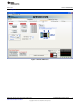
Launch AFE5809 GUI 6 www.ti.com Launch AFE5809 GUI Launch the AFE5809 graphic user interface (GUI), Figure 4. After successful launch, the status bar at the bottom should say "Ready for new command". Then, LED41 and LED42 turn off and the rest of the LEDS remain on. The GUI automatically configures the default setup. Select the ADC page to observe the default condition. Figure 4.
Launch AFE5809 GUI www.ti.com Figure 5 shows the Default Condition on the ADC window. Figure 5.
Launch TSW1400 GUI 7 www.ti.com Launch TSW1400 GUI Launch the TSW1400 GUI. A Pop-up window should prompt you to connect to the EVM if it is connected via USB. If a different message or an error message appears, contact the TI FAE. If the GUI connects properly, the status at the bottom says "Connected" in Green. Select AFE5809_09_14b for the firmware by clicking the blue arrow. Click Yes to update firmware on the board. This can take about 30 seconds.
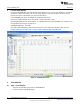
TEST AFE5809 www.ti.com Figure 7. TSW1400 GUI Configuration • From the AFE5809 GUI, go to the ADC page, and then select Ramp. • Press the Capture button on the TSW1400 GUI. This displays a ramping waveform on the TSW1400 GUI display area as shown in Figure 8. Verify that Maximum value is 16383 for 14-bit mode. Repeat for Channel 2 and Channel 8. If each channel has the output as shown in Figure 8, proceed with the next step; otherwise, contact the TI FAE to troubleshoot the problem.
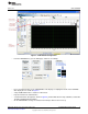
TEST AFE5809 www.ti.com Figure 8. Ramp Waveform Output 8.2 Step 2: Single Tone FFT • • • • • • • 10 Select Frequency from the display control on the TSW1400 GUI to display the FFT. Connect Channel 1 of the AFE5809EVM to a signal generator through a BP filter. If a BP filter is not present, the result is not good. Set the amplitude of the signal generator to -25 dBm. Set the frequency of the signal generator to the value in the "ADC Input Target Frequency" field of the TSW GUI.
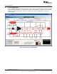
TEST AFE5809 www.ti.com Figure 9. GUI: Single FFT Format 8.3 Step 3: Demodulator Mode The AFE5809 has a special demodulation and decimation mode whose main purpose is to reduce the LVDS data rate and improve overall system power efficiency. The device includes some built-in test modes to verify that demodulator block is working correctly.
TEST AFE5809 www.ti.com Figure 10. Hardware Setup for Demodulation Mode Capture First, setup an analog input waveform at 10 MHz and 20 cycles similar to Figure 11 (Tektronix AFG3102 is recommended). Adjust amplitude until there is no clipping of waveform. Figure 11.
TEST AFE5809 www.ti.com The ADC must be set to the proper configuration for Demodulation: • ADC format must be MSB First, 2's Complement • LVDS Rate must be set to 16X • Choose any demodulator test mode from the following buttons: Sine Test Mode, RF Test Mode, Coefficient Test Mode and Demod M=4 I/Q Test Mode. • For modes and options, load a text using "Exec CMD File". Figure 12.
TEST AFE5809 • www.ti.com Under Demod M=4 I/Q Test Mode, also look at the "Separate Data" tab to view the I/Q separated Data. Figure 13.
TEST AFE5809 www.ti.com Figure 14.
TEST AFE5809 www.ti.com Figure 15.
TEST AFE5809 www.ti.com Figure 16.
TEST AFE5809 www.ti.com Figure 17.
TEST AFE5809 www.ti.com Figure 18.
Hardware Setup, CW Mode 9 www.ti.com Hardware Setup, CW Mode Figure 19.
Hardware Setup, CW Mode www.ti.com 9.1 Step 1: Switch to CW Mode • • • Go to the CW Mode page. Check CW Mode Enable. Then LED41, LED42, and LED43 on AFE5809EVM all illuminate. Select 500 Ω for the gain control feedback resistor. Figure 20.
Hardware Setup, CW Mode 9.2 www.ti.com Step 2: Apply Input and Observe Outputs • • Apply an analog signal (2.51 M, –10 dBm) to any analog input SMA. The CW outputs (J12, J13) display the frequency I and Q signals at 10 kHz as shown in Figure 21. The GUI Gain Control Feedback Resistor can be used to vary the amplitude of the outputs. Figure 21.
Hardware Setup, CW Mode www.ti.com 9.3 External Clock for CW Mode The CW mode clocks can be supplied from J9 (X16/X8/X4/X1) and J10 (X1) using external signal generators. The manufacture default setup uses ON BOARD CLOCK, with which C154, C155, C156, and C157 are installed. To switch to an external clock, these four capacitors must be uninstalled and capacitors C49,C50,C52, and C53 must be installed. The following table shows the configuration for these eight capacitors. Table 1.
Hardware Setup, CW Mode www.ti.com Figure 23. External ADC Sampling Clock Configuration 4. If the generators for the ADC clock and input signal are synchronous, then choose Rectangular as the Windowing option; otherwise, use Hanning or Hamming. Notice the spectrum spreading with noncoherence. Figure 24.
Hardware Setup, CW Mode www.ti.com 5. The test procedure is the same for the CMOS ADC clock.
External Vcntl 10 www.ti.com External Vcntl • • JP15 needs to be reconfigured to short the leftmost two pins. A DC Voltage source is required to be connected to J14. Figure 25.
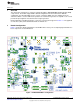
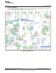
Board Configuration www.ti.com 11 Board Configuration 11.1 I/O, Power Supply, and USB Figure 26. I/O, PWR, and USB Connector Table 2. I/O, Power, and USB Connector Description J1 through J8 Analog Input signals for Ch1 through Ch8. Connect to a signal generator. A bandpass filter must be applied between the generator and the SMA to get a better result. (See Figure 1.) P1/JP6 P1 is the +5-V and –5-V power supply connector. JP6 is the test point for +5-V/-5-V power supply. JP3 Onboard 5-V enable.
Board Configuration www.ti.com Table 2. I/O, Power, and USB (continued) Connector Description TP33VD +3.3-VD supply test point TP33VA +3.3-VA supply test point TP14VD +1.4-VD supply test point TP1 through TP4 Ground test points USB1 USB interface connector P13,P14 Test points for USB data bus: From pin 1 to pin 9, the signals are D0, D4, D2, D1, D7, D5, D6, and D3 11.2 CW Mode, ADC Clock Figure 27.
Board Configuration www.ti.com Table 3. CW Mode, ADC Clock Clock Type Reference Designator Description J9/J10 External CW Mode clock. The default is using onboard oscillator. J12 JP52/JP53 CW Mode J13 JP56/JP57 ADC CW output for I-channel via an external operational amplifier. The EVM has converted the differential signal CW_IP_OUTP and CW_IP_OUTM into this single-ended output through an operational amplifier.
Board Configuration www.ti.com 11.4 LEDs The AFE5809EVM has seven LEDs. Their locations are shown in Figure 29. Their ON and OFF states demonstrate the normal operation of the power supplies and the PLL status of the clock buffer. Figure 29. AFE5809EVM LED Location Table 5. LED Indicators Reference Designator Power Supply Color LED-5V –5 V Green LED5V +5 V Green LED3.3VD +3.3 VD Orange LED3.3VA +3.3 VA Green LED1.8V +1.8 V Green LED_LDO +1.
Board Configuration www.ti.com 11.5 Miscellaneous Test Points Figure 30. AFE5809EVM Test Point Locations Table 6. Test Points Reference Designator Description TP11,TP14.TP15 AFE5809 device test pin DNC1, 2, and 3. Pins L5, M5 and M8 JP19 REFM voltage input JP44 RESET input. Short to reset AFE5809.
EVM Printed-Circuit Board Layouts and Schematics 12 www.ti.com EVM Printed-Circuit Board Layouts and Schematics Figure 31 through Figure 36 show the six layers of the AFE5809EVM board. Figure 31.
EVM Printed-Circuit Board Layouts and Schematics www.ti.com Figure 32.
EVM Printed-Circuit Board Layouts and Schematics www.ti.com Figure 33.
EVM Printed-Circuit Board Layouts and Schematics www.ti.com Figure 34.
EVM Printed-Circuit Board Layouts and Schematics www.ti.com Figure 35.
EVM Printed-Circuit Board Layouts and Schematics www.ti.com Figure 36.
EVM Printed-Circuit Board Layouts and Schematics www.ti.com 12.1 Schematics Power Figure 37.
EVM Printed-Circuit Board Layouts and Schematics www.ti.com AFE5809 DEVICE Figure 38.
EVM Printed-Circuit Board Layouts and Schematics www.ti.com VCA INPUT ADC OUTPUT Figure 39.
EVM Printed-Circuit Board Layouts and Schematics www.ti.com Clock Buffer Figure 40.
EVM Printed-Circuit Board Layouts and Schematics www.ti.com ADC CLOCK Figure 41.
EVM Printed-Circuit Board Layouts and Schematics www.ti.com CW CLK 16X 1X Figure 42.
EVM Printed-Circuit Board Layouts and Schematics www.ti.com VCON SINGLE TO DIFFERENTIAL CONVERTER Figure 43.
EVM Printed-Circuit Board Layouts and Schematics www.ti.com CW Mixer Out Figure 44.
EVM Printed-Circuit Board Layouts and Schematics www.ti.com Serial Interface There are two ground planes here. We isolate the USB circuit from the rest of the board. The circuits are only coupled through the opto-isolators. Figure 45.
EVM Printed-Circuit Board Layouts and Schematics www.ti.com CW I/V Amp ALL Bypass Caps in this circuit need to be tied close to the pin. This Circuit provides 3 options for populating Op-Amps for maximum flexibility Figure 46.
Bill of Materials 13 www.ti.com Bill of Materials Table 7.
Bill of Materials www.ti.com Table 7. Bill of Materials (continued) 14 7 AVX 0603YD105KAT2A C38, C39, C58, C63, C159, C161, C172 CAP,SMT,0603 CAPACITOR,SMT,0603,C ERAMIC,1.0uF,16V,10%,X 5R 15 1 TAIYO YUDEN AMK107BJ226MA-T C9 CAP,SMT,0603 CAPACITOR,SMT,0603,C ERAMIC,22uF,4V,20%,X5 R 16 1 PANASONIC ECJ-1VB0J106M C4 CAP,SMT,0603 CAPACITOR,SMT,0603,C ERAMIC,10uF,6.3V,20%,X 5R 17 3 PANASONIC ECJ-1VB1C105K C75, C93, C129 CAP,SMT,0603 CAPACITOR,SMT,0603,C ERAMIC,1.
Bill of Materials www.ti.com Table 7. Bill of Materials (continued) 30 1 MOLEX 39357-0003 P1 HEADER, THRU, 3P HEADER, THRU, POWER, 3P,3.5MM, EUROSTYLE 31 1 SAMTEC QTH-060-01-L-D-A P10 HEADER,SMT,120P HEADER,SMT,120P,0.
Bill of Materials www.ti.com Table 7. Bill of Materials (continued) 45 1 TI TPS79618DCQR U14 IC,SMT,SOT223-6 ULTRALOW-NOISE HI PSRR FAST RF 1-A LDO LINEAR REGULATOR,1.8V 46 2 TI TPS79633DCQR U1, U12 IC,SMT,SOT223-6 ULTRALOW-NOISE HI PSRR FAST RF 1-A LDO LINEAR REGULATOR,3.
Bill of Materials www.ti.com Table 7. Bill of Materials (continued) 63 6 PANASONIC ERJ-2GEJ820 R23, R24, R26, R27, R34 RES,SMT,0402 RESISTOR,SMT,0402,THI CK FILM,5%,1/16W,82 64 8 PANASONIC ERJ-2RKF1000X R25, R40, R42, R76, R78, R84, R85, R89 RES,SMT,0402 RESISTOR,SMT,0402,100 OHM,1%,1/10W 65 3 PANASONIC ERJ-2RKF3320X R59, R90, R94 RES,SMT,0402 RESISTOR,SMT,0402,332 OHM,1%,1/16W 66 3 PANASONIC ERJ-2RKF49R9X R83, R88, R96 RES,SMT,0402 RESISTOR,SMT,0402,49.
Bill of Materials www.ti.com Table 7. Bill of Materials (continued) 81 1 BOURNS 3296W-1-205 82 4 Digi-Key 83 4 84 VR1 TRIMPOT,THU,3P TRIMPOT,THU,2M,10%,0. 5W,100ppm,25T 29311K-ND SCREW STEEL M3 THR 6MM SCREW STEEL M3 THR 6MM Digi-Key 24436K-ND STANDOFF HEX M3 THR ALUM 18MM STANDOFF HEX M3 THR ALUM 18MM 20 Molex 15-29-1025 SHUNT-JUMPER CONN SHUNT CLOSED TOP .100 GOLD 85 2 SUSUMU RG1005N152B R10, R64 RES,SMT,0402 RESISTOR,SMT,0402,THI N FILM,1.5 K,0.
Bill of Materials www.ti.com Table 7. Bill of Materials (continued) 97 1 VISHAY CRCW04024701F100 R45 RES,SMT,0402 RESISTOR,SMT,0402,4.7 K,1/16W,1%,100ppm (UNINSTALLED) 98 1 ADVANCED CONNECTEK MNE20-5K5P10 USB1 CONN,SMT,5P MINI-AB USB OTG RECEPTACLE R/A SMT TYPE Use 670-1523-1-ND instead. 99 7 EFJOHNSON EFJOHNSON J2, J4, J6, J8, J14, J15, J17 CONN,THU,SMA JACK SMA JACK END LAUNCH, 0.080 PCB THICK. Use J630-ND for board thickness of .042 or J502ND for .062 or J992-ND for .
EVALUATION BOARD/KIT/MODULE (EVM) ADDITIONAL TERMS Texas Instruments (TI) provides the enclosed Evaluation Board/Kit/Module (EVM) under the following conditions: The user assumes all responsibility and liability for proper and safe handling of the goods. Further, the user indemnifies TI from all claims arising from the handling or use of the goods.
FCC Interference Statement for Class B EVM devices This equipment has been tested and found to comply with the limits for a Class B digital device, pursuant to part 15 of the FCC Rules. These limits are designed to provide reasonable protection against harmful interference in a residential installation. This equipment generates, uses and can radiate radio frequency energy and, if not installed and used in accordance with the instructions, may cause harmful interference to radio communications.
【Important Notice for Users of this Product in Japan】 】 This development kit is NOT certified as Confirming to Technical Regulations of Radio Law of Japan If you use this product in Japan, you are required by Radio Law of Japan to follow the instructions below with respect to this product: 1. 2. 3. Use this product in a shielded room or any other test facility as defined in the notification #173 issued by Ministry of Internal Affairs and Communications on March 28, 2006, based on Sub-section 1.
EVALUATION BOARD/KIT/MODULE (EVM) WARNINGS, RESTRICTIONS AND DISCLAIMERS For Feasibility Evaluation Only, in Laboratory/Development Environments. Unless otherwise indicated, this EVM is not a finished electrical equipment and not intended for consumer use.
IMPORTANT NOTICE Texas Instruments Incorporated and its subsidiaries (TI) reserve the right to make corrections, enhancements, improvements and other changes to its semiconductor products and services per JESD46, latest issue, and to discontinue any product or service per JESD48, latest issue. Buyers should obtain the latest relevant information before placing orders and should verify that such information is current and complete.