
Datasheet


AM26C31
www.ti.com
SLLS103N – DECEMBER 1990– REVISED OCTOBER 2011
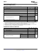
ELECTRICAL CHARACTERISTICS
over recommended ranges of supply voltage and operating free-air temperature (unless otherwise noted)
AM26C31C
AM26C31I
PARAMETER TEST CONDITIONS UNIT
MIN TYP
(1)
MAX
V
OH
High-level output voltage I
O
= –20 mA 2.4 3.4 V
V
OL
Low-level output voltage I
O
= 20 mA 0.2 0.4 V
V
OD
Differential output voltage magnitude R
L
= 100 Ω, See Figure 1 2 3.1 V
Δ|V
OD
| Change in magnitude of differential output voltage
(2)
R
L
= 100 Ω, See Figure 1 ±0.4 V
V
OC
Common-mode output voltage R
L
= 100 Ω, See Figure 1 3 V
Δ|V
OC
| Change in magnitude of common-mode output voltage
(2)
R
L
= 100 Ω, See Figure 1 ±0.4 V
I
I
Input current V
I
= V
CC
or GND ±1 μA
V
O
= 6 V 100
I
O(off)
Driver output current with power off V
CC
= 0 μA
V
O
= –0.25 V –100
I
OS
Driver output short-circuit current V
O
= 0 –30 –150 mA
V
O
= 2.5 V 20
I
OZ
High-impedance off-state output current μA
V
O
= 0.5 V –20
V
I
= 0 or 5 V 100 μA
I
CC
Quiescent supply current I
O
= 0
V
I
= 2.4 V or 0.5
1.5 3 mA
V
(3)
C
i
Input capacitance 6 pF
(1) All typical values are at V
CC
= 5 V and T
A
= 25°C.
(2) Δ|V
OD
| and Δ|V
OC
| are the changes in magnitude of V
OD
and V
OC
, respectively, that occur when the input is changed from a high level
to a low level.
(3) This parameter is measured per input. All other inputs are at 0 or 5 V.
SWITCHING CHARACTERISTICS
over recommended ranges of supply voltage and operating free-air temperature (unless otherwise noted)
AM26C31C
AM26C31I
PARAMETER TEST CONDITIONS UNIT
MIN TYP
(1)
MAX
t
PLH
Propagation delay time, low-to-high-level output 3 7 12
S1 is open, See Figure 2 ns
t
PHL
Propagation delay time, high-to-low-level output 3 7 12
t
sk(p)
Pulse skew time (|t
PLH
– t
PHL
|) S1 is open, See Figure 2 0.5 4 ns
t
r(OD)
, t
f(OD)
Differential output rise and fall times S1 is open, See Figure 3 5 10 ns
t
PZH
Output enable time to high level 10 19
S1 is closed, See Figure 4 ns
t
PZL
Output enable time to low level 10 19
t
PHZ
Output disable time from high level 7 16
S1 is closed, See Figure 4 ns
t
PLZ
Output disable time from low level 7 16
C
pd
Power dissipation capacitance (each driver)
(2)
S1 is open, See Figure 2 170 pF
(1) All typical values are at V
CC
= 5 V and T
A
= 25°C.
(2) C
pd
is used to estimate the switching losses according to P
D
= C
pd
× V
CC
2
× f, where f is the switching frequency.
Copyright © 1990–2011, Texas Instruments Incorporated Submit Documentation Feedback 5
Product Folder Link(s): AM26C31