
Datasheet


Enable G Input
(see Note C)
Output WIth
0 V to A Input
V
OL
+ 0.3 V
t
PLZ
t
PHZ
t
PZH
t
PZL
C3 =
40 pF
C2 =
40 pF
C1 =
40 pF
Input A
50 Ω
50 Ω
500 Ω
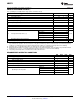
TEST CIRCUIT
VOLTAGE WAVEFORMS
3 V
0 V
1.5 V
V
OL
V
OH
V
OH
- 0.3 V
1.5 V
See Note A
G
G
Enable G Input
Output
Output
Output WIth
3 V to A Input
Enable Inputs
(see Note B)
0 V
3 V
1.5 V
S1
1.3 V1.3 V
2 V
0.8 V
AM26C31
SLLS103N –DECEMBER 1990–REVISED OCTOBER 2011
www.ti.com
PARAMETER MEASUREMENT INFORMATION (continued)
Figure 3. Differential-Output Rise- and Fall-Time Waveforms and Test Circuit
A. C1, C2, and C3 include probe and jig capacitance.
B. All input pulses are supplied by generators having the following characteristics: PRR ≤ 1 MHz, duty cycle ≤ 50%, and
t
r
, t
f
≤ 6 ns.
C. Each enable is tested separately.
Figure 4. Output Enable- and Disable-Time Waveforms and Test Circuit
8 Submit Documentation Feedback Copyright © 1990–2011, Texas Instruments Incorporated
Product Folder Link(s): AM26C31