
Datasheet


Input A
(see Note B)
Output Y
1.3 V
50%
t
sk(p)
Output Z
t
PHL
t
PLH
t
sk(p)
t
PLH
t
PHL
C3 = 40 pF
C2 = 40 pF
C1 =
40 pF
Input
See Note A
TEST CIRCUIT
R
L
/2
R
L
/2
1.5 V
500 Ω
S1
1.3 V
1.3 V
3 V
0 V
50%
50%
50%
AM26C31
www.ti.com
SLLS103N – DECEMBER 1990– REVISED OCTOBER 2011
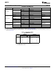
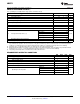
PARAMETER MEASUREMENT INFORMATION
Figure 1. Differential and Common-Mode Output Voltages
A. C1, C2, and C3 include probe and jig capacitance.
B. All input pulses are supplied by generators having the following characteristics: PRR ≤ 1 MHz, duty cycle ≤ 50%, and
t
r
, t
f
≤ 6 ns.
Figure 2. Propagation Delay Time and Skew Waveforms and Test Circuit
A. C1, C2, and C3 include probe and jig capacitance.
B. All input pulses are supplied by generators having the following characteristics: PRR ≤ 1 MHz, duty cycle ≤ 50%, and
t
r
, t
f
≤ 6 ns.
Copyright © 1990–2011, Texas Instruments Incorporated Submit Documentation Feedback 7
Product Folder Link(s): AM26C31