
Datasheet
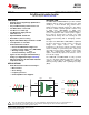
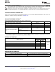
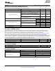

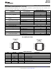
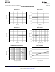
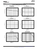
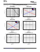
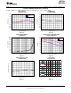
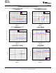
Table Of Contents
- FEATURES
- APPLICATIONS
- DESCRIPTION
- ABSOLUTE MAXIMUM RATINGS
- THERMAL INFORMATION
- REGULATORY INFORMATION
- IEC 60747-5-2 INSULATION CHARACTERISTICS
- IEC SAFETY LIMITING VALUES
- IEC 61000-4-5 RATINGS
- IEC 60664-1 RATINGS
- PACKAGE CHARACTERISTICS
- ELECTRICAL CHARACTERISTICS
- PIN CONFIGURATIONS
- TYPICAL CHARACTERISTICS
- THEORY OF OPERATION
- APPLICATION INFORMATION
- ISOLATION GLOSSARY
- REVISION HISTORY

1
2
3
4
8
7
6
5
VDD2
VOUTP
VOUTN
GND2
VDD1
VINP
VINN
GND1
1
2
3
4
8
7
6
5
VDD2
VOUTP
VOUTN
GND2
VDD1
VINP
VINN
GND1
AMC1200
AMC1200B
www.ti.com
SBAS542C –APRIL 2011–REVISED SEPTEMBER 2013
ELECTRICAL CHARACTERISTICS (continued)
All minimum/maximum specifications at T
A
= –40°C to +105°C and within the specified voltage range, unless otherwise noted.
Typical values are at T
A
= +25°C, VDD1 = 5 V, and VDD2 = 3.3 V.
AMC1200, AMC1200B
PARAMETER TEST CONDITIONS MIN TYP MAX UNIT
Rise/fall time 0.5-V step, 10% to 90% 3.66 6.6 µs
0.5-V step, 50% to 10%, unfiltered output 1.6 3.3 µs
V
IN
to V
OUT
signal delay 0.5-V step, 50% to 50%, unfiltered output 3.15 5.6 µs
0.5-V step, 50% to 90%, unfiltered output 5.26 9.9 µs
Common-mode transient
CMTI V
CM
= 1 kV 10 15 kV/µs
immunity
2.7 V ≤ VDD2 ≤ 3.6 V 1.15 1.29 1.45 V
Output common-mode voltage
4.5 V ≤ VDD2 ≤ 5.5 V 2.4 2.55 2.7 V
Short-circuit current 20 mA
R
OUT
Output resistance 2.5 Ω
POWER SUPPLY
VDD1 High-side supply voltage 4.5 5.0 5.5 V
VDD2 Low-side supply voltage 2.7 5.0 5.5 V
I
DD1
High-side supply current 5.4 8 mA
2.7 V < VDD2 < 3.6 V 3.8 6 mA
I
DD2
Low-side supply current
4.5 V < VDD2 < 5.5 V 4.4 7 mA
P
DD1
High-side power dissipation 27.0 44.0 mW
2.7 V < VDD2 < 3.6 V 11.4 21.6 mW
P
DD2
Low-side power dissipation
4.5 V < VDD2 < 5.5 V 22.0 38.5 mW
PIN CONFIGURATIONS
DUB PACKAGE
DWV PACKAGE
SOP-8
SOIC-8
(TOP VIEW)
(TOP VIEW)
PIN DESCRIPTIONS
PIN # PIN NAME FUNCTION DESCRIPTION
1 VDD1 Power High-side power supply
2 VINP Analog input Noninverting analog input
3 VINN Analog input Inverting analog input
4 GND1 Power High-side analog ground
5 GND2 Power Low-side analog ground
6 VOUTN Analog output Inverting analog output
7 VOUTP Analog output Noninverting analog output
8 VDD2 Power Low-side power supply
Copyright © 2011–2013, Texas Instruments Incorporated Submit Documentation Feedback 5
Product Folder Links: AMC1200 AMC1200B