
Datasheet
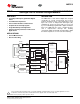


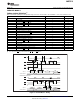

PARALLEL MODE 3
TIMING CHARACTERISTICS
(1)
ADDR
ADDR
ADDR+1
MSB LSB MSB
t
w5
t
d5
t
su1
t
h1
t
su2
t
h2
t
d1
t
d2
t
d3
t
d4
t
w4
t
w3
t
w1
t
w2
AD(7:0)
Internaladdress
Parallelmode3,writeaccess
CS
RD
WR
ALE
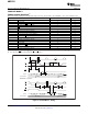
ADDR
ADDR
ADDR+1
MSB
LSB
MSB
t
d8
t
d6
t
d7
AD(7:0)
Internaladdress
Parallelmode3,readaccess
CS
RD
WR
ALE
AMC1210
SBAS372D – APRIL 2006 – REVISED MAY 2009 ..............................................................................................................................................................
www.ti.com
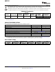
Over recommended operating free-air temperature range at – 40 ° C to +125 ° C, DVDD = +5V, and BVDD = +2.7V, unless otherwise noted.
PARAMETER
(2)
MIN MAX UNIT
t
w1
CS low width 40 ns
t
w2
CS high width 5 ns
t
d1
Delay time from WR low to CS low 5 ns
t
d2
Delay time from ALE high to CS high 5 ns
t
d3
Delay time from RD high to CS high 5 ns
t
d4
Delay time from CS low to RD low 3 ns
t
w3
RD low width 10 ns
t
w4
RD high width 30 ns
t
w5
ALE low width 6 ns
t
d5
Delay time from ALE high to RD low 10 ns
t
su1
Setup time from address valid to ALE high 5 ns
t
h1
Hold time from ALE high to address invalid 5 ns
t
su2
Setup time from data valid to RD high 5 ns
t
h2
Hold time from RD high to data invalid 5 ns
t
d6
Delay time from RD low to data valid 30 ns
t
d7
Delay time from RD high to databus in tristate 0 10 ns
t
d8
Delay time from WR high to CS low 5 ns
(1) All input signals are specified with t
R
= t
F
= 5ns (10% to 90% of BVDD) and timed from a voltage level of (V
IL
+ V
IH
)/2.
(2) t
w2
is obsolete if CS stays low between the RD and ALE pulses.
Figure 6. Parallel Mode 3 Timing
10 Submit Documentation Feedback Copyright © 2006 – 2009, Texas Instruments Incorporated
Product Folder Link(s): AMC1210