
Datasheet
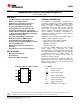


bq2000
www.ti.com
SLUS138D –JANUARY 2008–REVISED DECEMBER 2009
ABSOLUTE MAXIMUM RATINGS
(1)
VALUE UNIT
V
CC
V
CC
relative to V
SS
–0.3 to 7 V
V
T
DC voltage applied on any pin, relative to V
SS
–0.3 to V
CC
V
T
OPR
Operating ambient temperature –20 to 70 °C
T
STG
Storage temperature –40 to 125 °C
T
SOLDER
Soldering temperature (10 s max.) 260 °C
(1) Permanent device damage may occur if Absolute Maximum Ratings are exceeded. Functional operation should be limited to the
Recommended DC Operating Conditions detailed in this data sheet. Exposure to conditions beyond the operational limits for extended
periods of time may affect device reliability.
DC THRESHOLDS
(1)
T
A
= T
OPR
; V
CC
= 5V ±20% (unless otherwise specified)
PARAMETER TEST CONDITIONS TYPICAL TOLERANCE UNIT
V
TCO
Temperature cutoff Voltage at the TS pin 0.225 × V
CC
±5% V
V
HTF
High-temperature fault Voltage at the TS pin 0.25 × V
CC
±5% V
V
LTF
Low-temperature fault Voltage at the TS pin 0.5 × V
CC
±5% V
V
MCV
Maximum cell voltage Voltage at the BAT pin 2.00 ±0.75% V
V
LBAT
Minimum cell voltage Voltage at the BAT pin 950 ±5% mV
PVD BAT input change for PVD detection Voltage at the BAT pin 3.8 ±20% mV
V
SNSHI
High threshold at SNS Voltage at the SNS pin 50 ±10 mV
V
SNSLO
Low threshold at SNS Voltage at the SNS pin –50 ±10 mV
V
SLP
Sleep-mode input threshold Voltage at the BAT pin V
CC
–1 ±0.5 V
V
RCH
Recharge threshold Voltage at the BAT pin V
MCV
–0.1 ±0.02 V
(1) All voltages are relative to V
SS
except as noted.
RECOMMENDED DC OPERATING CONDITIONS
over operating free-air temperature range (unless otherwise noted)
TEST CONDITIONS MIN TYP MAX UNIT
V
CC
Supply voltage 4 5 6 V
I
CC
Supply current Exclusive of external loads 0.5 1 mA
I
CCS
Sleep current V
BAT
= V
SLPM
5 µA
V
TS
Thermistor input V
TS
< 0.5 V prohibited 0.5 VCC V
V
OH
Output high input MOD, I
OH
= 10 mA V
CC
–0.4 V
V
OL
Output low input MOD, LED, I
OL
= 10 mA 0.2 V
I
OZ
High-impedance leakage current LED 5 µA
I
snk
Sink current MOD, LED 20 mA
R
MTO
Charge timer resistor 2 250 kΩ
C
MTO
Charge timer capacitor 0.001 1 µF
IMPEDANCE
PARAMETER MIN TYP MAX UNIT
R
BAT
Battery input impedance 10 MΩ
R
TS
TS input impedance 10 MΩ
R
SNS
SNS input impedance 10 MΩ
TIMING
T
A
= T
OPR
; V
CC
= 5 V ±20% (unless otherwise noted)
PARAMETER MIN TYP MAX UNIT
d
MTO
MTO time-base variation –5% 5%
f
TRKL
Pulse-trickle frequency 0.9 1 1.1 Hz
Copyright © 2008–2009, Texas Instruments Incorporated Submit Documentation Feedback 5
Product Folder Link(s): bq2000