
Datasheet
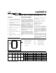


Pin Descriptions
TM
Timer mode input
A three-level input that controls the settings
for the fast charge safety timer, voltage ter
-
mination mode, top-off, pulse-trickle, and
voltage hold-off time.
LED
Charging output status
Open-drain output that indicates the charging
status.
BAT
Battery input voltage
The battery voltage sense input. The input to
this pin is created by a high-impedance re
-
sistor divider network connected between
the positive and negative terminals of the
battery.
V
SS
System ground
TS
Temperature sense input
Input for an external battery temperature
monitoring thermistor.
V
CC
Supply voltage input
5.0V
±
20%power input.
INH
Charge inhibit input
When high, INH suspends the fast charge in
progress. When returned low, the IC re-
sumes operation at the point where initially
suspended.
CC
Charge control output
An open-drain output used to control the
charging current to the battery. CC switch
-
ing to high impedance (Z) enables charging
current to flow, and low to inhibit charging
current. CC is modulated to provide top-off,
ifenabled,and pulse trickle.
Functional Description
Figure 2 shows a state diagram and Figure 3 shows a
block diagram ofthe bq2002E/G.
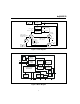
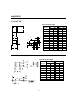
Battery Voltage and Temperature
Measurements
Battery voltage and temperature are monitored for
maximum allowable values. The voltage presented on
the battery sense input, BAT, should represent a
single-cell potential for the battery under charge. A
resistor-divider ratio of
RB1
RB2
= N - 1
is recommended to maintain the battery voltage within
the valid range, where N is the number of cells, RB1 is
the resistor connected to the positive battery terminal,
and RB2 is the resistor connected to the negative bat-
tery terminal. See Figure 1.
Note:
This resistor-divider network input impedance to
end-to-end should be at least 200k
Ω
and less than 1 M
Ω
.
2
bq2002E/G
Fg2002E/G01.eps
bq2002E/G
BAT
V
SS
N
T
C
bq2002E/G
V
CC
V
CC
PACK +
T
S
V
SS
BAT pin connection Thermistor connection
TM
NTC = negative temperature coefficient thermistor.
RT
R3
R4
RB1
RB2
Mid-level
setting for TM
Figure 1. Voltage and Temperature Monitoring and TM Pin Configuration