
Datasheet


7
bq2002E/G
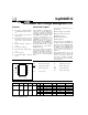
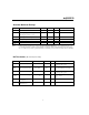
Absolute Maximum Ratings
Symbol Parameter Minimum Maximum Unit Notes
V
CC
V
CC
relative to V
SS
-0.3 +7.0 V
V
T
DC voltage applied on any pin
excluding V
CC
relative to V
SS
-0.3 +7.0 V
T
OPR
Operating ambient temperature 0 +70 °C Commercial
T
STG
Storage temperature -40 +85 °C
T
SOLDER
Soldering temperature - +260 °C 10 sec max.
T
BIAS
Temperature under bias -40 +85 °C
Note:
Permanent device damage may occur if
Absolute Maximum Ratings
are exceeded. Functional opera
-
tion should be limited to the Recommended DC Operating Conditions detailed in this data sheet. Expo
-
sure to conditions beyond the operational limits for extended periods of time may affect device reliability.
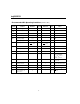
DC Thresholds (T
A
= 0 to 70°C; V
CC
±
20%)
Symbol Parameter Rating Tolerance Unit Notes
V
TCO
Temperature cutoff 0.5
*
V
CC
±
5% V V
TS
≤
V
TCO
inhibits/terminates
fast charge and top-off
V
HTF
High temperature fault
0.6
∗
VCC
±
5%
VV
TS
<V
HTF
inhibits fast charge
start
V
MCV
Maximum cell voltage 2
±
5% V
V
BAT
≥
V
MCV
inhibits/terminates
fast charge and top-off
V
LBAT
Minimum cell voltage
0.175
∗
V
CC
±
20%
VV
BAT
<V
LBAT
inhibits fast charge
start
-
∆
V
BAT input change for
-
∆
V detection
-12
±
3
mV
PVD BAT input change for
PVD detection
-2.5
±
2.5
mV