
Datasheet


Pin Descriptions
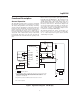
LCOM
LED common
This open-drain output switches V
CC
to source
current for the LEDs. The switch is off during
initialization to allow reading of PROG
1-5
pull-up or pull-down program resistors. LCOM
is also high impedance when the display is off.
SEG
1
–
SEG
5
LED display segment outputs (dual func-
tion with PROG
1
–PROG
5
Each output may activate an LED to sink
the current sourced from LCOM.
PROG
1
–
PROG
6
Programmed full count selection inputs
(dual function with SEG
1
- SEG
5
)
These three-level input pins define the pro-
grammed full-count (PFC), display mode,
self-discharge rate, offset compensation,
overload threshold, and charge compensa-
tion.
SR
Sense resistor input
The voltage drop (V
SR
) across the sense re-
sistor R
S
is monitored and integrated over
time to interpret charge and discharge activ-
ity. The SR input (see Figure 1) is connected
between the negative terminal of the battery
and ground. V
SR
>V
SS
indicates charge, and
V
SR
<V
SS
indicates discharge. The effective
voltage drop, V
SRO
, as seen by the bq2013H
is V
SR
+V
OS.
DONE
Charge complete input
This input/output is used to communicate
the status of an external charge controller to
the bq2013H.
DISP
Display control input
DISP
pulled high disables the display.
DISP
floating allows the LED display to
be active during certain charge and dis-
charge conditions. Transitioning DISP
low activates the display.
SB
Secondary battery input
This input monitors the scaled battery volt-
age through a high-impedance resistive di-
vider network for the end-of-discharge volt-
age (EDV) thresholds.
RBI
Register backup input
This input is used to provide backup poten-
tial to the bq2013H registers during periods
when V
CC
< 3V. A storage capacitor can be
connected to RBI.
HDQ
Serial I/O pin
This is an open-drain bidirectional commu-
nications port.
REF
Voltage reference output for regulator
REF provides a voltage reference output for
an optional micro-regulator.
V
CC
Supply voltage input
V
SS
Ground
2
bq2013H