
Datasheet


2
®
BUF634
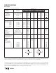
SPECIFICATIONS
ELECTRICAL
The information provided herein is believed to be reliable; however, BURR-BROWN assumes no responsibility for inaccuracies or omissions. BURR-BROWN
assumes no responsibility for the use of this information, and all use of such information shall be entirely at the user’s own risk. Prices and specifications are subject
to change without notice. No patent rights or licenses to any of the circuits described herein are implied or granted to any third party. BURR-BROWN does not
authorize or warrant any BURR-BROWN product for use in life support devices and/or systems.
V+
V–
V
O
V
IN
BW
V+
V–
V
O
V
IN
✻ Specifications the same as Low Quiescent Mode.
NOTES: (1) Tests are performed on high speed automatic test equipment, at approximately 25°C junction temperature. The power dissipation of this product will
cause some parameters to shift when warmed up. See typical performance curves for over-temperature performance. (2) Limited output swing available at low supply
voltage. See Output voltage specifications. (3) Typical when all leads are soldered to a circuit board. See text for recommendations.
At T
A
= +25°C
(1)
, V
S
= ±15V, unless otherwise noted.
BUF634P, U, T, F
LOW QUIESCENT CURRENT MODE WIDE BANDWIDTH MODE
PARAMETER CONDITION MIN TYP MAX MIN TYP MAX UNITS
INPUT
Offset Voltage ±30 ±100 ✻✻ mV
vs Temperature Specified Temperature Range ±100 ✻ µV/°C
vs Power Supply V
S
= ±2.25V
(2)
to ±18V 0.1 1 ✻✻mV/V
Input Bias Current V
IN
= 0V ±0.5 ±2 ±5 ±20 µA
Input Impedance R
L
= 100Ω 80 || 8 8 || 8 MΩ || pF
Noise Voltage f = 10kHz 4 ✻ nV/√Hz
GAIN R
L
= 1kΩ, V
O
= ±10V 0.95 0.99 ✻✻ V/V
R
L
= 100Ω, V
O
= ±10V 0.85 0.93 ✻✻ V/V
R
L
= 67Ω, V
O
= ±10V 0.8 0.9 ✻✻ V/V
OUTPUT
Current Output, Continuous ±250 ✻ mA
Voltage Output, Positive I
O
= 10mA (V+) –2.1 (V+) –1.7 ✻✻ V
Negative I
O
= –10mA (V–) +2.1 (V–) +1.8 ✻✻ V
Positive I
O
= 100mA (V+) –3 (V+) –2.4 ✻✻ V
Negative I
O
= –100mA (V–) +4 (V– ) +3.5 ✻✻ V
Positive I
O
= 150mA (V+) –4 (V+) –2.8 ✻✻ V
Negative I
O
= –150mA (V–) +5 (V–) +4 ✻✻ V
Short-Circuit Current ±350 ±550 ±400 ✻ mA
DYNAMIC RESPONSE
Bandwidth, –3dB R
L
= 1kΩ 30 180 MHz
R
L
= 100Ω 20 160 MHz
Slew Rate 20Vp-p, R
L
= 100Ω 2000 ✻ V/µs
Settling Time, 0.1% 20V Step, R
L
= 100Ω 200 ✻ ns
1% 20V Step, R
L
= 100Ω 50 ✻ ns
Differential Gain
3.58MHz, V
O
= 0.7V, R
L
= 150Ω
4 0.4 %
Differential Phase
3.58MHz, V
O
= 0.7V, R
L
= 150Ω
2.5 0.1 °
POWER SUPPLY
Specified Operating Voltage ±15 ✻ V
Operating Voltage Range ±2.25
(2)
±18 ✻✻V
Quiescent Current, I
Q
I
O
= 0 ±1.5 ±2 ±15 ±20 mA
TEMPERATURE RANGE
Specification –40 +85 ✻✻°C
Operating –40 +125 ✻✻°C
Storage –55 +125 ✻✻°C
Thermal Shutdown
Temperature, T
J
175 ✻ °C
Thermal Resistance,
θ
JA
“P” Package
(3)
100 ✻ °C/W
θ
JA
“U” Package
(3)
150 ✻ °C/W
θ
JA
“T” Package
(3)
65 ✻ °C/W
θ
JC
“T” Package 6 ✻ °C/W
θ
JA
“F” Package
(3)
65 ✻ °C/W
θ
JC
“F” Package 6 ✻ °C/W