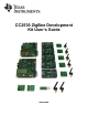
CC2530 ZigBee Development Kit User’s Guide swru209b
swru209b Table of contents CC2530 ZIGBEE DEVELOPMENT KIT USER’S GUIDE ............................................................................. 1 1 INTRODUCTION..................................................................................................................................... 3 2 ABOUT THIS MANUAL ......................................................................................................................... 3 3 ACRONYMS ........................................................
swru209b 1 Introduction Thank you for purchasing the CC2530 ZigBee Development Kit. The CC2530 is Texas Instrument’s second generation ZigBee/IEEE 802.15.4 compliant System-onChip with an optimized 8051 MCU core and radio for the 2.4 GHz unlicensed ISM/SRD band. This device enables industrial grade applications by offering state-of-the-art noise immunity, excellent link budget, operation up to 125 degrees and low voltage operation.
swru209b 3 Acronyms ACM BB CDC DK EB EM HID IC ISM KB LCD LED LPRF MCU NC PER RF RX SoC SPI SRD TI TX UART USB ZDK Z-Stack Abstract Control Model Battery Board Communications Device Class Development Kit Evaluation Board Evaluation Module Human Interface Device Integrated Circuit Industrial, Scientific and Medical Kilo Byte (1024 byte) Liquid Crystal Display Light Emitting Diode Low Power RF Micro Controller Not connected Packet Error Rate Radio Frequency Receive System on Chip Serial Peripheral Interfa
swru209b 4 ZigBee Development Kit contents The CC2530 ZigBee Development Kit (CC2530ZDK) includes hardware and software that allows quick testing of the CC2530 RF performance and offers a complete platform for development of advanced prototype RF systems and ZigBee applications. Evaluate the CC2530 and ZigBee right out of the box. The kit can be used to demonstrate a small sensor network application using ZigBee and the CC2530.
swru209b SmartRF05EB The SmartRF05EB (evaluation board) is the main board in the kit with a wide range of user interfaces: 3x16 character serial LCD Full speed USB 2.0 interface UART LEDs Serial Flash Potentiometer Joystick Buttons The EB is the platform for the evaluation modules (EM) and can be connected to the PC via USB to control the EM.
swru209b 5 Getting started 5.1 Setting up the hardware After opening the kit, make sure you have all components. Please contact your TI Sales Representative or TI Support [17] if anything is missing. Start by connecting the antennas to the SMA connector on the RF evaluation boards. Tighten the antenna’s screw firmly on to the SMA connector. If not properly connected, you might see reduced RF performance. It is also possible to connect the EM board to RF instruments via coax cables.
swru209b External regulated power source (not included in this kit) The power source can be selected using jumper P11 on the SmartRF05EB. The SmartRF05EB User’s Guide [6] provides more details. The SmartRF05 Battery Boards (BB) can be used as a standalone device when equipped with a CC2530EM. This board is powered by AA batteries. See section 10 in this document for more information about the SmartRF05BB. After assembling the hardware, you now have several options for working with the CC2530: 5.
swru209b PC. SmartRF Studio also offers a flexible code export function of radio register settings for software developers. Before proceeding, please download and install the latest version of SmartRF Studio from the web [2]. By installing Studio, the USB drivers needed for proper interaction between the PC and the hardware of the CC2530DK will also be installed. In order to use the SmartRF Studio with CC2530, connect the CC2530EM to the SmartRF05EB.
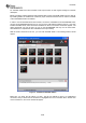
swru209b Figure 4 - CC2530 control panel in SmartRF Studio Figure 4 shows the main control panel for the CC2530. It lets you perform a number of operations: Run TX Test modes for testing of RF output power and spectrum; e.g. by connecting a spectrum analyser or a power meter to the CC2530EM SMA connector to perform RF measurements. Run Packet TX and RX tests. For this test, you should have two EBs with CC2530EMs connected to the PC.
swru209b 5.5 Developing your own software with the CC2530 To develop software and debug an application on the CC2530, it is recommended to use IAR Embedded Workbench. It supports debugging of CC2530 through the SmartRF05EB, so no additional hardware is required.
swru209b 6 RF Testing NB! When running RF performance tests, it is recommended to disable all other peripherals on the SmartRF05EB in order to avoid unwanted noise on the on-board voltage. In particular, make sure the RS232 level converter/line driver is disabled. RF testing can be performed by using SmartRF Studio together with the Development Kit. The basic set-up is described in section 5.4.
swru209b 6.2 RX Parameter Testing Basics To investigate the RX performance of the CC2530, you can use a signal generator or “Packet TX” in SmartRF Studio (with another EB+EM) to generate the packets to receive. The receiver can be configured by using the “Packet RX” test feature in SmartRF Studio.
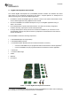
swru209b 7 CC2530EM SMA antenna connector 32 kHz Crystal 32MHz Crystal CC2530F256 EM Connector P1 (Bottom side) EM Connector P2 (Bottom side) Figure 6 - CC2530 Evaluation Module The CC2530EM is a complete RF module based on one of the recommended reference designs for the CC2530 radio. The module is equipped with a 32 MHz crystal, a 32.
swru209b 8 CC2531 USB Dongle Meandred F-antenna IO Connector CC2531F256 LEDs Button S2 Button S1 Debug connector Voltage regulator Figure 7 - CC2531 USB Dongle The USB dongle that is included in the kit comes preprogrammed such that it can be used together with the SmartRF Packet Sniffer [4] to capture packets going over the air. To use the dongle as a sniffer, just install the Packet Sniffer PC application (available on the web [4]), plug in the USB dongle and start capturing packets.
swru209b Figure 8 - CC2531 USB Dongle connected to SmartRF05EB The debug connector on the CC2531 USB Dongle matches the debug connector on the SmartRF05EB (and the CC Debugger). Note that, by default, the CC2531 dongle is not powered through the debug connector, so an external power source must be used while programming. The easiest solution is to connect it to a USB port on the PC. Alternatively, resistor R2 can be mounted. The table below shows the pin out of the debug connector.
swru209b 9 SmartRF05 Evaluation Board The SmartRF05 Evaluation Board is thoroughly described in the SmartRF05EB User’s Guide [6]. That document will describe the hardware features in detail and provide the schematics for the board.
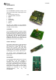
swru209b 10 SmartRF05 Battery Board 256kB SPI Flash Module EM Connectors LEDs Joystick Probe Connectors EM Selection Switch Power Switch Push Buttons Figure 9 SmartRF05 Battery Board The SmartRF05 Battery Board is a smaller and simpler board than the SmartRF05EB. The Battery Board can together with an EM be used as a standalone node. Figure 9 shows the SmartRF05 Battery Board. The Battery Board is powered with 2 AA batteries placed in the battery connectors underneath the board.
swru209b 10.1 Joystick The joystick detects five positions (centre, up, down, left, right) and one event (pushed). The two aggregated signals, JOY_MOVE and JOY_LEVEL, are used to detect a joystick event when using a SoC (e.g. the CC2530). JOY_MOVE is high whenever the joystick is moved away from the centre position, including pushing. The other signal, JOY_LEVEL, is a voltage level signal that gives different values depending on the current position of the joystick. The table below shows these values.
swru209b Function on BB Pin Pin Function on BB JOYSTICK_PUSH 1 2 GND NC 3 4 IO_LED2_MSP Not in use on BB 5 6 IO_LED3_MSP VCC_EM 7 8 IO_LED4_MSP VCC_EM 9 10 NC JOYSTICK_UP 11 12 Not in use on BB JOYSTICK_LEFT 13 14 Not in use on BB SoC Debug P3.7 & Flash Reset 15 16 IO_BUTTON2 Not in use on BB 17 18 Not in use on BB JOY_MOVE 19 20 Not in use on BB Table 6 EM connector P2 pin out 10.
swru209b Figure 11 - Switch P8 effect on LED 1-4 Due to lack of pins, some of the signals are shared. The chip select signal to the EM will also be affected when LED3 is used by the SoC (e.g. CC2530). In most cases, this will not be a problem, since the SoC does not, by default, implement a SPI slave. When LED4 is used by the SoC, the signal from Button 1 might interfere. In short, Button 1 and LED 4 can not be used simultaneously by the SoC.
swru209b 10.4 Probe connectors The probe connectors P4 and P5 bring out all the signals from the EM connectors for probing purposes. The connectors allow easy access to I/O signals and to connect prototyping boards. The pin-out of these connectors are shown below. Function on BB Signal name Pin Pin Signal name Function on BB NC NC 1 2 NC NC Not in use on BB EM_P2_14 3 4 EM_P1_04 FLASH_CS 5 6 EM_P1_13 IO_LED2_SOC 7 8 EM_P1_10 SoC Debug P3.4 9 10 EM_P1_12 SoC Debug P3.
swru209b Figure 13 Program/debug with SmartRF05EB The pin out of this connector is depicted below. For debugging and programming of the SoC the following signals are used; SoC RESET_N, DD and DC. In addition GND and +3.3V shall be connected. Figure 14 SmartRF05BB SoC Debug Connector As seen on Figure 14 also the SPI signals CS, MISO, MOSI and SCLK can be found on this connector. 10.
swru209b 11 Frequently Asked Questions Q1 When connecting the SmartRF05EB to my PC via USB, the dialog window below appears. Why? What should I do? A1 The SmartRF05EB will be recognized as a USB device by the operating system, and it will ask the user to provide information about which USB driver that should be associated with the device. If you have installed SmartRF Studio, just follow the instructions and select “Automatic installation”. Windows should find the required driver (cebal2.
swru209b Q3 How can I measure the current consumption of the CC2530? A3 The easiest way to measure current consumption of the chip in various modes is to connect the EM directly to the SmartRF05EB and disconnect everything on the board that consumes power by removing all jumpers. The jumper on header P13 should not be removed. Connect the ampere meter between the two terminals on P15. On P10, the jumper for the EM_RESET signal (connector 35-36) should be mounted.
swru209b 12 References [1] CC2530 product web site http://focus.ti.com/docs/prod/folders/print/cc2530.html [2] SmartRF Studio product web site http://focus.ti.com/docs/toolsw/folders/print/smartrftm-studio.html [3] SmartRF Flash Programmer product web site http://focus.ti.com/docs/toolsw/folders/print/flash-programmer.html [4] SmartRF Packet Sniffer http://focus.ti.com/docs/toolsw/folders/print/packet-sniffer.html [5] SmartRF Packet Sniffer User Manual http://www.ti.
swru209b 13 Document history Revision Date B 2011-04-05 A - 2009-08-04 2009-06-08 Description/Changes Clarified that IAR EW8051 is required when working with the Z-Stack. Updated screenshots of SmartRF Studio. Include updated schematics. Fixed a few typos. Added SmartRF05 Battery Board schematics First revision.
swru209b Appendix A Schematics Please refer to the following pages for the schematics for CC2530 Evaluation Module CC2531 USB Dongle SmartRF05 Evaluation Board SmartRF05 Battery Board The reference design for the CC2530 evaluation module can be found on the CC2530 web page [1].
2 C311 C_100N_0402_X5R_K_10 2 1 C272 C_220P_0402_NP0_J_50 2 1 C271 C_100N_0402_X5R_K_10 2 1 C241 C_100N_0402_X5R_K_10 2 1 C211 C_100N_0402_X5R_K_10 1 C101 C_100N_0402_X5R_K_10 2 C391 C_1U_0402_X5R_K_6P3 1 1 2 FIDUCIAL_MARK FM4 FIDUCIAL_MARK FM2 FIDUCIAL_MARK FM5 FIDUCIAL_MARK FM3 FIDUCIAL_MARK FM6 VDD L1 L_BEAD_102_0402 1 FIDUCIAL_MARK FM1 2 1 2 C1 C_2U2_0402_X5R_M_4VDC CC2530_TX_REDES 1 2 3 P1 SMD_SOCKET_2X10 4 AVDD1 AVDD4 AVDD_GUARD 27 28 18 17 16 15 P0.6 13 P0.
FIDUCIAL_MARK_1mm FIDUCIAL_MARK_1mm FM1 FM2 FIDUCIAL_MARK_1mm FM3 1 1 1 VOLTAGE REGULATOR SoC periferials Generated voltage: 3.3 V for CC2531 RF-SoC PART Including PCB antenna - USB Connector Buttons LEDs SMD sockets RESET_N RESET_N P0_0 P0_0 P0_2 P0_3 P0_4 P0_5 P0_2 P0_3 P0_4 P0_5 P1_0/LED P1_1/LED P1_2 P1_3 P1_4 P1_5 P1_6 P1_7 P2_1 P2_2 PA_DM PA_DP P1_0/LED P1_1/LED P1_2 P1_3 P1_4 P1_5 P1_6 P1_7 P2_1 P2_2 PA_DM PA_DP CONTRACT NO.
To CC2531 VCC_EXT 3.3V 1 From PC U2 TPS76933 R3 R_0_0402 1 In Out VREG C1 C_1U_0603_X5R_L_6P3 1 /EN NC 1 Gnd 2 R2 R_0402 VBUS C3 C_0402 1 2 2 C2 C_4U7_0603_X5R_K_6 2 2 1 R1 R_2_0402_F 2 Not mount: C3, R2 CONTRACT NO. 025104 APPROVALS DATE DRAWN TIK CHECKED MAP ISSUED COMPANY NAME Texas Instruments DWG CC2531 USB DONGLE VOLTAGE REGULATOR SIZE FSCM NO. DWG NO. SCALE REV. 2.
VCC L1 L_BEAD_102_0402 2 1 2 1 2 C311 C_100N_0402_X5R_K_10 2 1 C272 C_220P_0402_NP0_J_50 1 C271 C_100N_0402_X5R_K_10 2 C241 C_100N_0402_X5R_K_10 1 2 2 C211 C_100N_0402_X5R_K_10 2 1 C101 C_100N_0402_X5R_K_10 1 C391 C_1U_0402_X5R_K_6P3 1 C41 C_10P_0402_NP0_J_50 1 3.
USB Interface LED_Red R11 R_270_0402_F 3.3V 1 2 R92 R_0402 2 R32 R_1K5_0402_G 2 R71 R_270_0402_F P1_0/LED P0_0 1 2 PA_DM D+ 3 1 2 PA_DP GND 4 Shield 6 2 3.
PCB_FEET_19 H3 Power Supply USB Interface - Regulators - Power jumpers - Battery - CC2511 - CC2511 debug - USB port PCB_FEET_19 H2 USB_UART_RTS USB_UART_CTS USB_UART_RX USB_UART_TX PCB_FEET_19 H1 USB_DBG_DD_DIR USB_DBG_DC USB_DBG_DD USB_CS USB_MISO USB_MOSI USB_SCLK PCB_FEET_19 H4 USB MCU IO jumpers VCC_IO Sheet 4 USB_IO_RESET USB_EM_RESET USB_JOY_MOVE JOYSTICK_UP JOYSTICK_DN JOYSTICK_LT JOYSTICK_RT JOYSTICK_PUSH JOY_MOVE JOY_LEVEL Sheet 2 - EM connection - External SoC debug EM_DBG_DD EM_
+3.3V USB USB SoC Debug USB BUTTON +3.3V USB VCC_IO L4 +3.
VCC_IO SN74AVC4T245 1 VCCA VCCB 2 1DIR 3 2DIR 4 1B1 1A1 5 1B2 1A2 6 2B1 2A1 7 2B2 2A2 8 GND GND EM_DBG_DD_DIR EM_DBG_DD EM_RESET EM_DBG_DC External SOC Debug 16 15 14 13 12 11 10 9 DUT_VCC PINROW_2X5 P3 1 2 3 4 5 6 7 8 9 10 DUT_DD PINROW_SMD_2X5_1.27MM P4 1 2 DUT_VCC 3 4 DUT_DD 5 6 7 8 9 10 DUT_VCC DUT_DD VCC_EM 2 SMD_HEADER_2x10 P5 1 2 3 4 5 6 7 8 9 10 11 12 13 14 15 16 17 18 19 20 2 1 C29 2 Mount 0 ohm resistor in position R30 to power DUT from +3.
2 LPS3015-222ML 2 L1 1 U4 1 R34 2 5 R_0_0603 1 C9 2 C_100N_0603_X7R_K_50 R45 R_1M0_0603_J 1 2 C_4U7_0805_X5R_K_25 8 6 1 C38 7 9 2 TPS63030 VCC_EM jumper L1 L2 VIN VOUT 2 STRAP_1 1 P15 1 R68 R_1M0_0603_J 2 1 VINA EN FB PS/SYNC PGND GND PPAD 10 3 11 1 2 1 2 2 VCC_EM C11 C_10U_0805_X5R_K_10 4 2.
BUTTON1_POWER_MSP LCD VCC_IO P19 Switch_6pin VCC_IO 1 1 R16 1 2 15 IO_LCD_MODE 4 7 9 12 BUTTON1_POWER_SOC R_0_0603 R8 VCC_IO U10 SN74CBTLV3257PW 2 VDD 1B1 3 GND 1B2 5 2B1 S 6 IO_LED1 IO_LED2_MSP IO_LED2_SOC 2B2 OE 1A 3B1 2A 3B2 3A 4B1 4A 4B2 11 10 14 13 IO_LED3_MSP IO_LED3_SOC IO_LED4_MSP IO_BUTTON1/IO_LED4_SOC VCC_IO S1 PUSH_BUTTON 8 SN74ALVC14 U11-D 2 Yellow R21 R_10K_0603_G 2 BUTTON1_POWER_MSP C_100N_0603_X7R_K_50 2 1 1 R_270_0603_J Vss BUTTON 1 1 R39 2 IO_MISO
R28 R_0_0603 C1+ V+ VCC GND C1FORCEON R2OUTB R1OUT R2OUT R3OUT R4OUT R5OUT 28 27 26 25 24 23 22 21 20 19 18 17 16 15 1 C25 C_100N_0603_X7R_K_50 2 1 C24 C_100N_0603_X7R_K_50 VCC_IO 2 R46 R_0_0603 1 4 5 6 C2+ C2VR1IN R2IN R3IN R4IN R5IN T1OUT T2OUT T3OUT T3IN T2IN T1IN 1 U6 SN65C3243DBR 1 2 3 4 5 6 7 8 9 10 11 12 13 14 1 C15 2 3 2 2 1 C14 2 2 EM_UART_RX P16 DSUB_9F Switch_6pin P14 2 C23 C_100N_0603_X7R_K_50 C_1U_0603_X5R_K_10 C22 C_100N_0603_X7R_K_50 1 C_100N_0603_X7R_K_50 1 1 2
UP JOYSTICK LT R61 R_0_0603 CENTRE push 2 JOYSTICK_RT 4 VCC_IO 5 1 COMMON left down C D 1 C31 C_100N_0603_X7R_K_50 2 U1 skrhab_e010 3 6 DN 2 R59 R_0_0603 2 JOYSTICK_DN R26 R_100K_0603_F 1 2 1 2 1 R_100K_0603_F R25 JOYSTICK_LT 1 2 2 R58 R_0_0603 1 B right 2 1 R24 R_100K_0603_F JOYSTICK_PUSH A up PUSH RT 1 2 1 1 R62 R_0_0603 R22 R_100K_0603_F 2 R_100K_0603_F R23 JOYSTICK_UP 1 2 R57 R_0_0603 U7-A SN74HC32 U7-B SN74HC32 1 U7-C SN74HC32 34 2 U7-D SN74HC32 10 6
IMPORTANT NOTICE Texas Instruments Incorporated and its subsidiaries (TI) reserve the right to make corrections, modifications, enhancements, improvements, and other changes to its products and services at any time and to discontinue any product or service without notice. Customers should obtain the latest relevant information before placing orders and should verify that such information is current and complete.