User Guide 2014 CC3100BOOST (CC3100 Booster Pack) User Guide, Ver 1.1 ECS Applications ABSTRACT ABSTRACT This This document document describes describes the the CC3100BOOST CC3100BOOST (CC3100 (CC3100 Booster Booster Pack). Pack). It It details details the the features features of the hardware and also explains the correct usage of the board. of the hardware and also explains the correct usage of the board.
CC3100BOOST User Guide TABLE OF CONTENTS 1 Introduction ................................................................................................................................ 4 2 Overview ...................................................................................................................................... 4 3 Hardware description ................................................................................................................ 4 3.1 Board overview .............
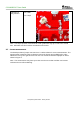
CC3100BOOST User Guide TI Proprietary Information - Strictly Private
CC3100BOOST User Guide 1 Introduction This document provides a quick start guide on using the CC3100 Booster Pack Rev 2.0B . This is not applicable to other revisions of the board. 2 Overview The CC3100 Booster Pack is a board designed to interface with the TI standard Launchpad including the Tiva-C series and the MSP430 value line launchpads. In addition to the launchpads, there is support available to mate the board with a FTDI Debug board to interface directly to a PC host using USB cable.
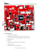
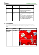
CC3100BOOST User Guide Antenna U.FL RF SIGNAL SELECT SERIAL FLASH CC3100 Sense on Power RESET USB CONN GPIO13 TOP DIE FLASH Vcc RESET BUTTON CC3100 Vcc GPIO12 Current Measurement FIGURE 1 : HARDWARE DETAILS 3.2 Board features 2x20 pin stackable connectors On-board chip antenna with option for U.FL based conducted testing. Power from on-board LDO using USB OR 3.3V from MCU Launchpad Push buttons (2x) LEDs (4x) Jumper with 0.1 Ohm resistor for current measurement. .
CC3100BOOST User Guide 4 Layer PCB with 6mil spacing and track width. 3.3 Jumper and connector information 3.3.1 2x20 pin connector The signal assignment on the 2x20 pin connector is shown below. The convention of J1..J4 is replaced with P1…P4 to avoid confusion with the actual board reference. Outer row connectors Pin No P1.1 P1.2 P1.3 P1.4 P1.5 P1.6 P1.7 P1.8 P1.9 P1.10 Signal Name VCC(3.
CC3100BOOST User Guide For the SPI lines, the CC3100 always acts like a slave. 3.4 Jumper details Reference Usage Comments J5 USB connector For powering the booster pack when mated with a Launchpad J6 Power selection Choose the power supply from the Lauchpad or the on-board USB. J6 (1-2) power from MCU Launchpad J6 (2-3) power from on-board USB using 3.3V LDO J24 Current measurement Voltage is measured across the 0.1 Ohm resistor using a voltmeter. Can be used for IDLE and Active currents.
CC3100BOOST User Guide part with 3.3V LDO. Install this for all boards with the CC3100Z parts. J2 Sense on power Sense on power used for internal debug. SOP[2:0] = 000 [Functional 4W] SOP[2:0] = 001 [Functional 2W] SOP[2:0] = 010 [Load from EEPROM] SOP[2:0] = 011 [Boot Debug mode] SOP[2:0] = 100 [UART LOAD] SOP[2:0] = 101 [TESTMODE 3] SOP[2:0] = 110 [TESTMODE 2] SOP[2:0] = 111 [TESTMODE 1] J1 3.5 RF Test U.FL connector for conducted testing.
CC3100BOOST User Guide GPIO_08. LED glows when GPIO_08 goes low. D7 nHIB Green LED Glows when the CC3100 device is enabled using nHIB. D5 RED LED to indicate the power line status. Power Note : This LED can glow if the board is powered from any of the GPIO being high, and the Vcc is un-connected. This is not a valid state and should be avoided. 3.6 Conducted testing The board is by default configured for radiated measurement using the on-board chip antenna.
CC3100BOOST User Guide Radiated test using antenna C4 = DNP C2 = 10pF Note : The 10pF capacitor used should be of RF grade with high-Q to reduce the overall loss. Otherwise a 0 Ohm resistor can also be used for this. 3.7 Current measurement The board provides a jumper connected to a 0.1 Ohm resistor for current measurement. The measurement is made by using a voltmeter across the jumper and multiplying the value obtained in mV by 10 to get the current in mA.
CC3100BOOST User Guide 4 Connecting to a PC using FTDI Board FIGURE 2 : PC CONNECTION USING FTDI The image above shows the connection of the Booster Pack to the FTDI Board. The connectors should be aligned carefully considering that it does not have a polarity protection. The pin-1 of the connectors are marked on the board using a DOT and these should be aligned while mating. Note : The mating and unmating force needed for these connectors may be large and may end up breaking the boards.
CC3100BOOST User Guide 4 J23 (open) OOB demo jumper 5 SOP jumpers All open 6 J22 (shorted) RESET control from FTDI and BP button After installing these jumpers the board would resemble as below 4.2 Jumper settings on the FTDI Board The following table specifies the jumpers to be installed while mating with the FTDI board.
CC3100BOOST User Guide After installing the jumpers, the board would resemble below 4.3 FTDI Board details 4.3.1 Overview The FTDI Debug Board 2.0A is designed to connect the Booster pack to a PC using USB connection. This is used to update the firmware on the BP using the “SL_Prog” utility and also in software development using “SL_Studio”.
CC3100BOOST User Guide 4.3.2 Hardware details Power SPI, GPIO, UART, RT3 MAC and NWP Logger The board has two FTDI ICs to enumerate multiple COM and D2XX ports.
CC3100BOOST User Guide 3 VCP COM port for flash programming 4 VCP RT3 For RF debug using RT3 software Note : On the PC only two of the four ports would be visible on the Device Manager. The D2XX ports are not listed under the “Ports” tab. The first COM port in the list usually is used for the flash programming. For SL_Prog Ports available on J2 Port No Port Type Usage 1 VCP MAC logg UART Tx for WLAN Debug 2 VCP NWP log UART Tx for debugging Comments 4.3.
CC3100BOOST User Guide 5 Connecting to a Launchpad The CC3100 Booster pack can be directly connected to a compatible Launchpad using the standard 2x20 pin connectors. The jumper settings needed for this connection is the same as that needed for the FTDI Debug board as described in the previous section. Please ensure that the Pin1 of the 2x20 pins are aligned correctly before mating. The mated setup is as per the picture below. (Note the USB cable is connected to the Booster Pack directly to power it only.
CC3100BOOST User Guide FIGURE 4 : JUMPER SETTINGS WHEN USED WITH LAUNCHPAD Important : Since there are two power sources in this setup it is important to follow the power-up sequence. Note : Always power the Booster Pack before powering the Launchpad.
CC3100BOOST User Guide 5.2 Connecting to an experimenter’s board. The Boosterpack could be connected to an experimenters board like the MSP430 FRAM experimenter’s board using an EM Adapter board. The EM adapter board converts the EM connectors to the standard 2x20 pin connectors of the booster pack headers. The stacked setup is as shown below. Ensure that the connectors are oriented correctly before powering up the board.
CC3100BOOST User Guide TI Proprietary Information - Strictly Private
CC3100BOOST User Guide TI Proprietary Information - Strictly Private
CC3100BOOST User Guide TI Proprietary Information - Strictly Private