
Data Sheet
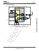
Table Of Contents
- 1 Module Overview
- Table of Contents
- 2 Revision History
- 3 Device Comparison
- 4 Terminal Configuration and Functions
- 5 Specifications
- 5.1 Absolute Maximum Ratings
- 5.2 ESD Ratings
- 5.3 Recommended Operating Conditions
- 5.4 Current Consumption Summary: 2.4 GHz RF Band
- 5.5 Current Consumption Summary: 5 GHz RF Band
- 5.6 TX Power Control for 2.4 GHz Band
- 5.7 TX Power Control for 5 GHz Band
- 5.8 Brownout and Blackout Conditions
- 5.9 Electrical Characteristics for DIO Pins
- 5.10 WLAN Receiver Characteristics
- 5.11 WLAN Transmitter Characteristics
- 5.12 BLE and WLAN Coexistence Requirements
- 5.13 Reset Requirement
- 5.14 Thermal Resistance Characteristics for MOB Package
- 5.15 Timing and Switching Characteristics
- 5.16 External Interfaces
- 6 Detailed Description
- 7 Applications, Implementation, and Layout
- 8 Environmental Requirements and SMT Specifications
- 9 Device and Documentation Support
- 10 Mechanical, Packaging, and Orderable Information
- Important Notice

TI Confidential – NDA Restrictions
ADVANCEINFORMATION
5
CC3135MOD
www.ti.com
SWRS225A –FEBRUARY 2019–REVISED AUGUST 2019
Submit Documentation Feedback
Product Folder Links: CC3135MOD
Table of ContentsCopyright © 2019, Texas Instruments Incorporated
Table of Contents
1 Module Overview ........................................ 1
1.1 Features .............................................. 1
1.2 Applications........................................... 2
1.3 Description............................................ 2
1.4 Functional Block Diagrams ........................... 3
2 Revision History ......................................... 6
3 Device Comparison ..................................... 7
3.1 Related Products ..................................... 8
4 Terminal Configuration and Functions.............. 9
4.1 CC3135MOD Pin Diagram ........................... 9
4.2 Pin Attributes ........................................ 10
4.3 Signal Descriptions.................................. 14
4.4 Connections for Unused Pins ....................... 16
5 Specifications........................................... 17
5.1 Absolute Maximum Ratings ......................... 17
5.2 ESD Ratings ........................................ 17
5.3 Recommended Operating Conditions............... 17
5.4 Current Consumption Summary: 2.4 GHz RF Band 18
5.5 Current Consumption Summary: 5 GHz RF Band .. 18
5.6 TX Power Control for 2.4 GHz Band................ 19
5.7 TX Power Control for 5 GHz Band.................. 21
5.8 Brownout and Blackout Conditions ................. 22
5.9 Electrical Characteristics for DIO Pins .............. 23
5.10 WLAN Receiver Characteristics .................... 24
5.11 WLAN Transmitter Characteristics.................. 25
5.12 BLE and WLAN Coexistence Requirements........ 26
5.13 Reset Requirement ................................. 26
5.14 Thermal Resistance Characteristics for MOB
Package ............................................. 26
5.15 Timing and Switching Characteristics ............... 27
5.16 External Interfaces .................................. 29
6 Detailed Description ................................... 33
6.1 Overview ............................................ 33
6.2 Module Features .................................... 33
6.3 Power-Management Subsystem .................... 37
6.4 Low-Power Operating Modes ....................... 38
6.5 Restoring Factory Default Configuration ............ 38
6.6 Hostless Mode ...................................... 39
6.7 Device Certification and Qualification ............... 40
6.8 Module Markings .................................... 42
6.9 End Product Labeling ............................... 43
6.10 Manual Information to the End User ................ 43
7 Applications, Implementation, and Layout ....... 44
7.1 Application Information .............................. 44
7.2 PCB Layout Guidelines ............................. 50
8 Environmental Requirements and SMT
Specifications........................................... 56
8.1 Temperature......................................... 56
8.2 Handling Environment .............................. 56
8.3 Storage Condition ................................... 56
8.4 PCB Assembly Guide ............................... 56
8.5 Baking Conditions................................... 57
8.6 Soldering and Reflow Condition .................... 58
9 Device and Documentation Support ............... 59
9.1 Device Nomenclature ............................... 59
9.2 Development Tools and Software................... 59
9.3 Firmware Updates................................... 60
9.4 Documentation Support ............................. 60
9.5 Trademarks.......................................... 61
9.6 Electrostatic Discharge Caution..................... 61
9.7 Export Control Notice ............................... 61
9.8 Glossary............................................. 61
10 Mechanical, Packaging, and Orderable
Information .............................................. 62
10.1 Mechanical, Land, and Solder Paste Drawings..... 62
10.2 Package Option Addendum ......................... 63