
User's Guide
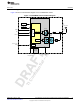


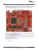

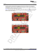
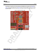
Table Of Contents
- CC3235MODSF SimpleLink™ Wi-Fi® and IoT Solution With MCU LaunchPad™ Hardware
- Table of Contents
- 1 Introduction
- 2 Hardware
- 2.1 Block Diagram
- 2.2 Hardware Features
- 2.2.1 Key Benefits
- 2.2.2 XDS110-Based Onboard Debug Probe
- 2.2.3 Debug Probe Connection: Isolation Jumper Block
- 2.2.4 Application (or "Backchannel") UART
- 2.2.5 JTAG Headers
- 2.2.6 Using the XDS110 Debug Probe with a Different Target
- 2.2.7 Power Connections
- 2.2.8 Reset Pullup Jumper
- 2.2.9 Clocking
- 2.2.10 I2C Connection
- 2.2.11 Sense on Power (SOP)
- 2.2.12 Push-Buttons and LED Indicators
- 2.3 Electrical Characteristics
- 2.4 Antenna Characteristics
- 2.5 BoosterPack™ Header Pin Assignment
- 3 Layout Guidelines
- 4 Operational Setup and Testing
- 5 Development Environment Requirements
- 6 Additional Resources
- 7 Assembly Drawing and Schematics
- Revision History
- Important Notice

TI Confidential – NDA Restrictions
www.ti.com
Hardware
13
SWRU548A–February 2019
Submit Documentation Feedback
Copyright © 2019, Texas Instruments Incorporated
CC3235MODSF LaunchPad™ Development Kit (LAUNCHCC3235MOD)
2.2 Hardware Features
• CC3235MODSF, SimpleLink
TM
Dual-Band Wi-Fi
®
module solution with integrated MCU
• 40-pin LaunchPad™ standard that leverages the BoosterPack™ ecosystem
• TI Standard XDS110-based JTAG emulation with serial port for flash programming
• Supports both 4-wire JTAG and 2-wire SWD
• Two buttons and a RGB LED for user interaction
• Virtual COM port UART through USB on PC
• Onboard chip antenna with U.FL or SMA for conducted testing, selectable using 0-Ω resistors
• Onboard accelerometer and temperature sensor for out-of-box demo, with the option to isolate them
from the inter-integrated circuit (I
2
C) bus
• Micro USB connector for power and debug connections
• Headers for current measurement and external JTAG connection, with an option to use the onboard
XDS110 to debug customer platforms
• Bus-powered device, with no external power required for Wi-Fi
®
• Long-range transmission with a highly optimized antenna (200-meter typical in open air with a 6-dBi
antenna AP)
• Can be powered externally, working down to 2.3 V
2.2.1 Key Benefits
The CC3235MODx modules offer the following benefits:
• Fully Integrated and Green/RoHS Modules Includes All Required Clocks, SPI Flash, and Passives
• 802.11 a/b/g/n: 2.4 GHz and 5 GHz
• FCC, IC/ISED, ETSI/CE, and MIC Certified
• FIPS 140-2 Level 1 Validated IC Inside
• Multilayered security features, help developers protect identities, data, and software IP
• Low-Power Modes for battery powered application
• Coexistence with 2.4 GHz Radios
• Industrial Temperature: –40°C to +85°C
• CC3235MODx Multiple-core architecture, system-on-chip (SoC)
• 1.27-mm Pitch QFM Package for Easy Assembly and Low-Cost PCB Design
• Transferrable Wi-Fi Alliance
®
Certification
• Application microcontroller subsystem:
– Arm
®
Cortex
®
-M4 core at 80 MHz
– User-dedicated memory
• 256 KB RAM
• Optional 1 MB executable Flash
– Rich set of peripherals and timers
– 26 I/O pins with flexible multiplexing options
• UART, I2S, I2C, SPI, SD, ADC, and 8-bit parallel interface
• 8-bit Synchronous Image Interface
• Timers and PWM
– Debug Interfaces: JTAG, cJTAG, and SWD