
User's Guide
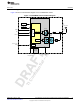


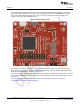

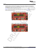
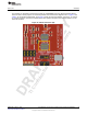
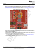
Table Of Contents
- CC3235MODSF SimpleLink™ Wi-Fi® and IoT Solution With MCU LaunchPad™ Hardware
- Table of Contents
- 1 Introduction
- 2 Hardware
- 2.1 Block Diagram
- 2.2 Hardware Features
- 2.2.1 Key Benefits
- 2.2.2 XDS110-Based Onboard Debug Probe
- 2.2.3 Debug Probe Connection: Isolation Jumper Block
- 2.2.4 Application (or "Backchannel") UART
- 2.2.5 JTAG Headers
- 2.2.6 Using the XDS110 Debug Probe with a Different Target
- 2.2.7 Power Connections
- 2.2.8 Reset Pullup Jumper
- 2.2.9 Clocking
- 2.2.10 I2C Connection
- 2.2.11 Sense on Power (SOP)
- 2.2.12 Push-Buttons and LED Indicators
- 2.3 Electrical Characteristics
- 2.4 Antenna Characteristics
- 2.5 BoosterPack™ Header Pin Assignment
- 3 Layout Guidelines
- 4 Operational Setup and Testing
- 5 Development Environment Requirements
- 6 Additional Resources
- 7 Assembly Drawing and Schematics
- Revision History
- Important Notice

TI Confidential – NDA Restrictions
www.ti.com
Hardware
17
SWRU548A–February 2019
Submit Documentation Feedback
Copyright © 2019, Texas Instruments Incorporated
CC3235MODSF LaunchPad™ Development Kit (LAUNCHCC3235MOD)
2.2.3 Debug Probe Connection: Isolation Jumper Block
The isolation jumper block at jumper J101 allows the user to connect or disconnect signals that cross from
the XDS110 domain into the CC3235MOD target domain. This includes JTAG signals, application UART
signals, and 3.3-V and 5-V power.
Reasons to open these connections:
• To remove any and all influence from the XDS110 debug probe for high accuracy target power
measurements
• To control 3-V and 5-V power flow between the XDS110 and target domains
• To expose the target MCU pins for other use than onboard debugging and application UART
communication
• To expose the programming and UART interface of the XDS110 so that it can be used for devices
other than the onboard MCU.
Table 1. Isolation Block Connections
Jumper Description
BRD Board Power. Supplies the board power from the onboard DC-DC converter. The board power
includes the sensors, LED, and the OPAMP used to drive the ADC input.
GND Ground reference
5V 5-V VBUS from USB
VBAT 3.3-V rail, derived from VBUS in the XDS110 domain. Can also be used to measure the current
flowing into the CC3235MOD.
RX Backchannel UART: The target CC3235MODSF receives data through this signal.
TX Backchannel UART: The target CC3235MODSF sends data through this signal.
RST This pin functions as the RST signal (active low).
TMS Serial wire data input (SWDIO) / JTAG test mode select (TMS)
TCK Serial wire clock input (SWCLK) / JTAG clock input (TCK)
TDO JTAG test data out
TDI JTAG test data in
VBUFFER Used to power the level shifters located on the emulator side of the board. The level shifters can
be powered by shorting this pin with a jumper. Removing the jumper enables low current
measurement.