
User's Guide
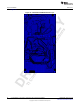
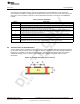

Table Of Contents
- CC3235MODSF SimpleLink™ Wi-Fi® and IoT Solution With MCU LaunchPad™ Hardware
- Table of Contents
- 1 Introduction
- 2 Hardware
- 2.1 Block Diagram
- 2.2 Hardware Features
- 2.2.1 Key Benefits
- 2.2.2 XDS110-Based Onboard Debug Probe
- 2.2.3 Debug Probe Connection: Isolation Jumper Block
- 2.2.4 Application (or "Backchannel") UART
- 2.2.5 JTAG Headers
- 2.2.6 Using the XDS110 Debug Probe with a Different Target
- 2.2.7 Power Connections
- 2.2.8 Reset Pullup Jumper
- 2.2.9 Clocking
- 2.2.10 I2C Connection
- 2.2.11 Sense on Power (SOP)
- 2.2.12 Push-Buttons and LED Indicators
- 2.3 Electrical Characteristics
- 2.4 Antenna Characteristics
- 2.5 BoosterPack™ Header Pin Assignment
- 3 Layout Guidelines
- 4 Operational Setup and Testing
- 5 Development Environment Requirements
- 6 Additional Resources
- 7 Assembly Drawing and Schematics
- Revision History
- Important Notice

TI Confidential – NDA Restrictions
www.ti.com
Layout Guidelines
33
SWRU548A–February 2019
Submit Documentation Feedback
Copyright © 2019, Texas Instruments Incorporated
CC3235MODSF LaunchPad™ Development Kit (LAUNCHCC3235MOD)
3.2 General Layout Recommendations
Ensure that the following general layout recommendations are followed:
• Have a solid ground plane and ground vias under the module for stable system and thermal
dissipation.
• Do not run signal traces underneath the module on a layer where the module is mounted.
3.3 RF Layout Recommendations
The RF section of this wireless module gets top priority in terms of layout. It is very important for the RF
section to be laid out correctly to ensure optimum performance from the module. A poor layout can cause
low-output power, EVM degradation, sensitivity degradation, and mask violations.
Figure 20 shows the RF placement and routing of the CC3235MODSF module.
Figure 20. RF Section Layout