
User's Guide
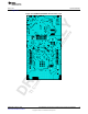
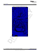
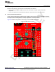
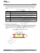

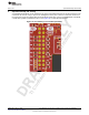
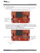
Table Of Contents
- CC3235MODSF SimpleLink™ Wi-Fi® and IoT Solution With MCU LaunchPad™ Hardware
- Table of Contents
- 1 Introduction
- 2 Hardware
- 2.1 Block Diagram
- 2.2 Hardware Features
- 2.2.1 Key Benefits
- 2.2.2 XDS110-Based Onboard Debug Probe
- 2.2.3 Debug Probe Connection: Isolation Jumper Block
- 2.2.4 Application (or "Backchannel") UART
- 2.2.5 JTAG Headers
- 2.2.6 Using the XDS110 Debug Probe with a Different Target
- 2.2.7 Power Connections
- 2.2.8 Reset Pullup Jumper
- 2.2.9 Clocking
- 2.2.10 I2C Connection
- 2.2.11 Sense on Power (SOP)
- 2.2.12 Push-Buttons and LED Indicators
- 2.3 Electrical Characteristics
- 2.4 Antenna Characteristics
- 2.5 BoosterPack™ Header Pin Assignment
- 3 Layout Guidelines
- 4 Operational Setup and Testing
- 5 Development Environment Requirements
- 6 Additional Resources
- 7 Assembly Drawing and Schematics
- Revision History
- Important Notice

TI Confidential – NDA Restrictions
Copyright © 2017, Texas Instruments Incorporated
Layout Guidelines
www.ti.com
34
SWRU548A–February 2019
Submit Documentation Feedback
Copyright © 2019, Texas Instruments Incorporated
CC3235MODSF LaunchPad™ Development Kit (LAUNCHCC3235MOD)
Use the following RF layout recommendations for the CC3235MODx module:
• RF traces must have 50-Ω impedance.
• RF trace bends must be made with gradual curves, and 90 degree bends must be avoided.
• RF traces must not have sharp corners.
• There must be no traces or ground under the antenna section.
• RF traces must have via stitching on the ground plane beside the RF trace on both sides.
• RF traces must be as short as possible. The antenna, RF traces, and the module must be on the edge
of the PCB product in consideration of the product enclosure material and proximity.
For optimal RF performance, ensure the copper cut out on the top layer under the RF-BG pin (pin 31) is
as shown in Figure 21.
Figure 21. Top Layer Copper Pullback on RF Pads