
User's Guide
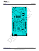
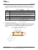

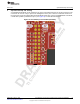
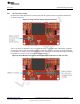
Table Of Contents
- CC3235MODSF SimpleLink™ Wi-Fi® and IoT Solution With MCU LaunchPad™ Hardware
- Table of Contents
- 1 Introduction
- 2 Hardware
- 2.1 Block Diagram
- 2.2 Hardware Features
- 2.2.1 Key Benefits
- 2.2.2 XDS110-Based Onboard Debug Probe
- 2.2.3 Debug Probe Connection: Isolation Jumper Block
- 2.2.4 Application (or "Backchannel") UART
- 2.2.5 JTAG Headers
- 2.2.6 Using the XDS110 Debug Probe with a Different Target
- 2.2.7 Power Connections
- 2.2.8 Reset Pullup Jumper
- 2.2.9 Clocking
- 2.2.10 I2C Connection
- 2.2.11 Sense on Power (SOP)
- 2.2.12 Push-Buttons and LED Indicators
- 2.3 Electrical Characteristics
- 2.4 Antenna Characteristics
- 2.5 BoosterPack™ Header Pin Assignment
- 3 Layout Guidelines
- 4 Operational Setup and Testing
- 5 Development Environment Requirements
- 6 Additional Resources
- 7 Assembly Drawing and Schematics
- Revision History
- Important Notice

TI Confidential – NDA Restrictions
www.ti.com
Layout Guidelines
35
SWRU548A–February 2019
Submit Documentation Feedback
Copyright © 2019, Texas Instruments Incorporated
CC3235MODSF LaunchPad™ Development Kit (LAUNCHCC3235MOD)
3.4 Antenna Placement and Routing
The antenna is the element used to convert the guided waves on the PCB traces to the free space
electromagnetic radiation. The placement and layout of the antenna are the keys to increased range and
data rates. Table 9 provides a summary of the recommended antennas to use with the CC3235MODx
module.
Table 9. Antenna Guidelines
SR NO. GUIDELINES
1 Place the antenna on an edge or corner of the PCB.
2 Ensure that no signals are routed across the antenna elements on all the layers of the PCB.
3
Most antennas, including the chip antenna used on the LaunchPad, require ground clearance on all the layers of
the PCB. Ensure that the ground is cleared on inner layers as well.
4
Ensure that there is provision to place matching components for the antenna. These must be tuned for best
return loss when the complete board is assembled. Any plastics or casing must also be mounted while tuning
the antenna because this can impact the impedance.
5 Ensure that the antenna impedance is 50 Ω because the module is rated to work only with a 50-Ω system.
6 In case of printed antenna, ensure that the simulation is performed with the solder mask in consideration.
7 Ensure that the antenna has a near omnidirectional pattern.
8
The feed point of the antenna is required to be grounded. This is only for the antenna type used on the
CC3235MODx LaunchPad. See the specific antenna data sheets for the recommendations.
3.5 Transmission Line Considerations
The RF signal from the module is routed to the antenna using a Coplanar Waveguide with ground (CPW-
G) structure. CPW-G structure offers the maximum amount of isolation and the best possible shielding to
the RF lines. In addition to the ground on the L1 layer, placing GND vias along the line also provides
additional shielding. Figure 22 shows a cross section of the coplanar waveguide with the critical
dimensions.
Figure 22. Coplanar Waveguide (Cross Section)