
User's Guide
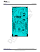
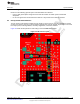
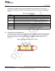

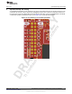
Table Of Contents
- CC3235MODSF SimpleLink™ Wi-Fi® and IoT Solution With MCU LaunchPad™ Hardware
- Table of Contents
- 1 Introduction
- 2 Hardware
- 2.1 Block Diagram
- 2.2 Hardware Features
- 2.2.1 Key Benefits
- 2.2.2 XDS110-Based Onboard Debug Probe
- 2.2.3 Debug Probe Connection: Isolation Jumper Block
- 2.2.4 Application (or "Backchannel") UART
- 2.2.5 JTAG Headers
- 2.2.6 Using the XDS110 Debug Probe with a Different Target
- 2.2.7 Power Connections
- 2.2.8 Reset Pullup Jumper
- 2.2.9 Clocking
- 2.2.10 I2C Connection
- 2.2.11 Sense on Power (SOP)
- 2.2.12 Push-Buttons and LED Indicators
- 2.3 Electrical Characteristics
- 2.4 Antenna Characteristics
- 2.5 BoosterPack™ Header Pin Assignment
- 3 Layout Guidelines
- 4 Operational Setup and Testing
- 5 Development Environment Requirements
- 6 Additional Resources
- 7 Assembly Drawing and Schematics
- Revision History
- Important Notice

TI Confidential – NDA Restrictions
www.ti.com
Operational Setup and Testing
39
SWRU548A–February 2019
Submit Documentation Feedback
Copyright © 2019, Texas Instruments Incorporated
CC3235MODSF LaunchPad™ Development Kit (LAUNCHCC3235MOD)
4.2 RF Connections
4.2.1 AP Connection Testing
By default, the board ships with the 2.4 GHz and 5 GHz RF signals routed to the onboard chip antenna,
as shown in Figure 25.
Figure 25. Using Onboard Antenna (Default Condition)
A U.FL connector J17 provides a way to test in the lab using a compatible cable. Alternatively, trackpads
for an SMA connector J15 are provided onboard to replace the J17 U.FL connector for testing conducted
measurements. A rework must be performed before these connectors can be used; this involves swapping
the position of a resistor. Figure 26 shows the modified board.
Figure 26. Board Modified for External Antenna Connections (Measure 2.4 GHz or 5 GHz)