
Datasheet


MOTOROLA CMOS LOGIC DATA
409
MC14518B MC14520B
The MC14518B dual BCD counter and the MC14520B dual binary counter
are constructed with MOS P–channel and N–channel enhancement mode
devices in a single monolithic structure. Each consists of two identical,
independent, internally synchronous 4–stage counters. The counter stages
are type D flip–flops, with interchangeable Clock and Enable lines for
incrementing on either the positive–going or negative–going transition as
required when cascading multiple stages. Each counter can be cleared by
applying a high level on the Reset line. In addition, the MC14518B will count
out of all undefined states within two clock periods. These complementary
MOS up counters find primary use in multi–stage synchronous or ripple
counting applications requiring low power dissipation and/or high noise
immunity.
• Diode Protection on All Inputs
• Supply Voltage Range = 3.0 Vdc to 18 Vdc
• Internally Synchronous for High Internal and External Speeds
• Logic Edge–Clocked Design — Incremented on Positive Transition of
Clock or Negative Transition on Enable
• Capable of Driving Two Low–power TTL Loads or One Low–power
Schottky TTL Load Over the Rated Temperature Range
MAXIMUM RATINGS* (Voltages Referenced to V
SS
)
Symbol
Parameter Value Unit
V
DD
DC Supply Voltage – 0.5 to + 18.0 V
V
in
, V
out
Input or Output Voltage (DC or Transient) 0.5 to V
DD
+ 0.5 V
I
in
, I
out
Input or Output Current (DC or Transient),
per Pin
± 10 mA
P
D
Power Dissipation, per Package† 500 mW
T
stg
Storage Temperature – 65 to + 150
C
T
L
Lead Temperature (8–Second Soldering) 260
C
* Maximum Ratings are those values beyond which damage to the device may occur.
†Temperature Derating:
Plastic “P and D/DW” Packages: – 7.0 mW/ C From 65 C To 125 C
Ceramic “L” Packages: – 12 mW/ C From 100 C To 125 C
TRUTH TABLE
Clock Enable Reset Action
1 0 Increment Counter
0 0 Increment Counter
X 0 No Change
X 0 No Change
0 0 No Change
1 0 No Change
X X 1 Q0 thru Q3 = 0
X = Don’t Care
SEMICONDUCTOR TECHNICAL DATA
Motorola, Inc. 1995
REV 3
1/94
L SUFFIX
CERAMIC
CASE 620
ORDERING INFORMATION
MC14XXXBCP Plastic
MC14XXXBCL Ceramic
MC14XXXBDW SOIC
T
A
= – 55° to 125°C for all packages.
P SUFFIX
PLASTIC
CASE 648
DW SUFFIX
SOIC
CASE 751G
This device contains protection circuitry to
guard against damage due to high static
voltages or electric fields. However, pre-
cautions must be taken to avoid applications of
any voltage higher than maximum rated volt-
ages to this high–impedance circuit. For proper
operation, V
in
and V
out
should be constrained
to the range V
SS
(V
in
or V
out
) V
DD
.
Unused inputs must always be tied to an
appropriate logic voltage level (e.g., either V
SS
or V
DD
). Unused outputs must be left open.
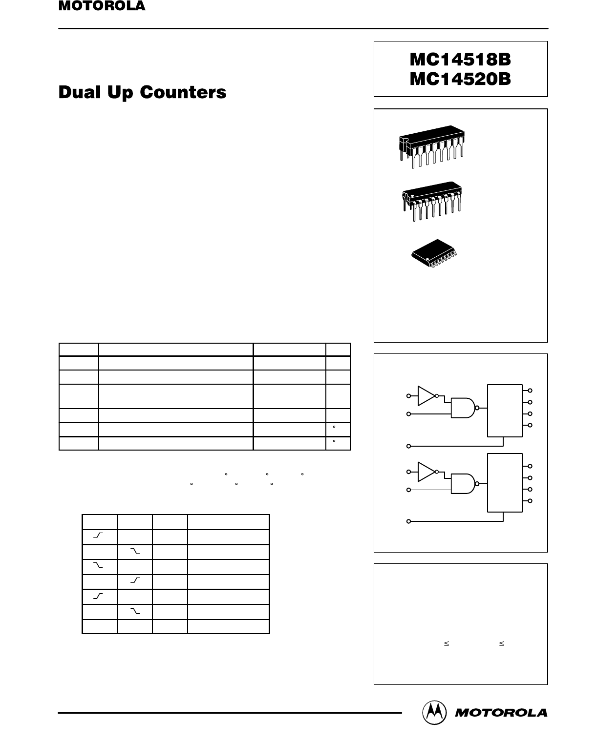
BLOCK DIAGRAM
V
DD
= PIN 16
V
SS
= PIN 8
3
4
5
6
14
13
12
11
C
C
R
R
Q3
Q2
Q1
Q0
Q3
Q2
Q1
Q0
CLOCK
1
2
CLOCK
ENABLE
ENABLE
7
9
10
15