
Datasheet


− 1 −
Data sheet acquired from Harris Semiconductor
SCHS211E
Features
¥ Buffered Inputs
¥ Separate Serial Outputs Synchronous to Both
Positive and Negative Clock Edges For Cascading
¥ Fanout (Over Temperature Range)
− Standard Outputs . . . . . . . . . . . . . . . 10 LSTTL Loads
− Bus Driver Outputs . . . . . . . . . . . . . 15 LSTTL Loads
¥ Wide Operating T emperature Rang e . . . −55
o
C to 125
o
C
¥ Balanced Propagation Delay and Transition Times
¥ Signi cant Power Reduction Compared to LSTTL
Logic ICs
¥ HC Types
− 2V to 6V Operation
− High Noise Immunity: N
IL
= 30%, N
IH
= 30% of V
CC
at V
CC
= 5V
¥ HCT Types
− 4.5V to 5.5V Operation
− Direct LSTTL Input Logic Compatibility,
V
IL
= 0.8V (Max), V
IH
= 2V (Min)
− CMOS Input Compatibility, I
l
≤
1
μ
A at V
OL
, V
OH
Description
The ÕHC4094and CD74HCT4094 are 8−stage serial shift
registers having a storage latch associated with each stage
for strobing data from the serial input to parallel buffered
three−stateoutputs. The parallel outputs may be connected
directly to common bus lines. Data is shifted on positive
clock transitions. The data in each shift register stage is
transferred to the storage register when the Strobe input is
high. Data in the storage register appears at the outputs
whenever the Output−Enable signal is high.
Two serial outputs are available for cascading a number of
these devices. Data is available at the QS
1
serial output
terminal on positive clock edges to allow for high−speed
operation in cascaded system in which the clock rise time is
fast. The same serial information, available at the QS
2
terminal on the next negative clock edge, provides a means
for cascading these devices when the clock rise time is slow.
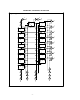
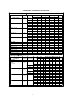
Pinout
CD54HC4094 (CERDIP)
CD74HC4094 (PDIP, SOIC, SOP, TSSOP)
CD74HCT4094 (PDIP, SOIC)
TOP VIEW
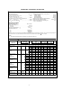
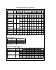
Ordering Information
PART NUMBER
TEMP. RANGE
(
o
C) PACKAGE
CD54HC4094F3A −55 to 125 16 Ld CERDIP
CD74HC4094E −55 to 125 16 Ld PDIP
CD74HC4094M −55 to 125 16 Ld SOIC
CD74HC4094MT −55 to 125 16 Ld SOIC
CD74HC4094M96G3 −55 to 125 16 Ld SOIC
CD74HC4094NSR −55 to 125 16 Ld SOP
CD74HC4094PW −55 to 125 16 Ld TSSOP
CD74HC4094PWR −55 to 125 16 Ld TSSOP
CD74HC4094PWT −55 to 125 16 Ld TSSOP
CD74HCT4094E −55 to 125 16 Ld PDIP
CD74HCT4094M −55 to 125 16 Ld SOIC
CD74HCT4094MT −55 to 125 16 Ld SOIC
CD74HCT4094M96 −55 to 125 16 Ld SOIC
NOTE: When ordering, use the entire part number. The suf xes 96
and R denote tape and reel. The suf x T denotes a small−quantity
reel of 250.
14
15
16
9
13
12
11
10
1
2
3
4
5
7
6
8
STROBE
DATA
CP
Q
0
Q
1
Q
2
GND
Q
3
V
CC
Q
4
Q
5
Q
6
Q
7
QS
2
QS
1
OE
November 1997 − Revised December 2010
CAUTION: These devices are sensitive to electrostatic discharge . Users should follow proper IC Handling Procedures.
Copyright 2003, Texas Instruments Incorporated
CD54HC4094, CD74HC4094,
CD74HCT4094
High−Speed CMOS Logic
8−Stage Shift and Store Bus Register, Three−State
[ /Title
(CD74H
C4094,
CD74H
CT4094
)
/Sub−
ject
(High
Speed
CMOS
Logic 8−