
Datasheet

SCHS279D − DECEMBER 1998 − REVISED OCTOBER 2003
1
POST OFFICE BOX 655303 • DALLAS, TEXAS 75265
D 2-V to 6-V V
CC
Operation (’HC4511)
D 4.5-V to 5.5-V V
CC
Operation
(CD74HCT4511)
D High-Output Sourcing Capability
− 7.5 mA at 4.5 V (CD74HCT4511)
− 10 mA at 6 V (’HC4511)
D Input Latches for BCD Code Storage
D Lamp Test and Blanking Capability
D Balanced Propagation Delays and
Transition Times
D Significant Power Reduction Compared to
LSTTL Logic ICs
D ’HC4511
− High Noise Immunity,
N
IL
or N
IH
= 30% of V
CC
at V
CC
= 5 V
D CD74HCT4511
− Direct LSTTL Input Logic Compatibility,
V
IL
= 0.8 V Maximum, V
IH
= 2 V Minimum
− CMOS Input Compatibility, I
I
≤ 1 µA
at V
OL
, V
OH
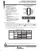
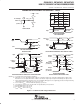
description/ordering information
The CD54HC4511, CD74HC4511, and CD74HCT4511 are BCD-to-7 segment latch/decoder/drivers with four
address inputs (D
0
−D
3
), an active-low blanking (BL) input, lamp-test (LT) input, and a latch-enable (LE) input
that, when high, enables the latches to store the BCD inputs. When LE
is low, the latches are disabled, making
the outputs transparent to the BCD inputs.
These devices have standard-size output transistors, but are capable of sourcing (at standard V
OH
levels) up
to 7.5 mA at 4.5 V. The HC types can supply up to 10 mA at 6 V.
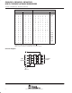
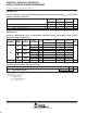
ORDERING INFORMATION
T
A
PACKAGE
†
ORDERABLE
PART NUMBER
TOP-SIDE
MARKING
PDIP − E
Tube of 25
CD74HC4511E CD74HC4511E
PDIP − E Tube of 25
CD74HCT4511E CD74HCT4511E
Tube of 40 CD74HC4511M
−55°C to 125°C
SOIC − M
Reel of 2500 CD74HC4511M96
HC4511M
−55°C to 125°C
SOIC − M
Reel of 250 CD74HC4511MT
HC4511M
TSSOP − PW
Reel of 2000 CD74HC4511PWR
HJ4511
TSSOP − PW
Reel of 250 CD74HC4511PWT
HJ4511
CDIP − F Tube of 25 CD54HC4511F3A CD54HC4511F3A
†
Package drawings, standard packing quantities, thermal data, symbolization, and PCB design
guidelines are available at www.ti.com/sc/package.
Copyright 2003, Texas Instruments Incorporated
!" # $%&" !# '%()$!" *!"&+
*%$"# $ " #'&$$!"# '& ",& "&# &-!# #"%&"#
#"!*!* .!!"/+ *%$" '$&##0 *&# " &$&##!)/ $)%*&
"&#"0 !)) '!!&"&#+
Please be aware that an important notice concerning availability, standard warranty, and use in critical applications of
Texas Instruments semiconductor products and disclaimers thereto appears at the end of this data sheet.
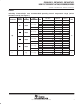
1
2
3
4
5
6
7
8
16
15
14
13
12
11
10
9
D
1
D
2
LT
BL
LE
D
3
D
0
GND
V
CC
f
g
a
b
c
d
e
BCD
Inputs
BCD
Inputs
7-Segment
Outputs
CD54HC4511 ...F PACKAGE
CD74HC4511 . . . E, M, OR PW PACKAGE
CD74HCT4511 ...E PACKAGE
(TOP VIEW)
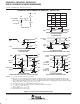
01 23 456789
DISPLAY
a
b
c
d
e
fg
'*%$"# $')!" " 1232 !)) '!!&"&# !& "&#"&*
%)&## ",&.#& "&*+ !)) ",& '*%$"# '*%$"
'$&##0 *&# " &$&##!)/ $)%*& "&#"0 !)) '!!&"&#+