
Datasheet
SEMICONDUCTOR
1
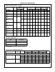
Features
• Buffered Inputs
• Separate Serial Outputs Synchronous to Both
Positive and Negative Clock Edges For Cascading
• Fanout (Over Temperature Range)
- Standard Outputs. . . . . . . . . . . . . . . 10 LSTTL Loads
- Bus Driver Outputs . . . . . . . . . . . . . 15 LSTTL Loads
• Wide Operating Temperature Range . . . -55
o
C to 125
o
C
• Balanced Propagation Delay and Transition Times
• Significant Power Reduction Compared to LSTTL
Logic ICs
• HC Types
- 2V to 6V Operation
- High Noise Immunity: N
IL
= 30%, N
IH
= 30% of V
CC
at V
CC
= 5V
• HCT Types
- 4.5V to 5.5V Operation
- Direct LSTTL Input Logic Compatibility,
V
IL
= 0.8V (Max), V
IH
= 2V (Min)
- CMOS Input Compatibility, I
l
≤ 1µA at V
OL
, V
OH
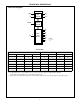
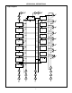
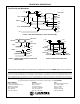
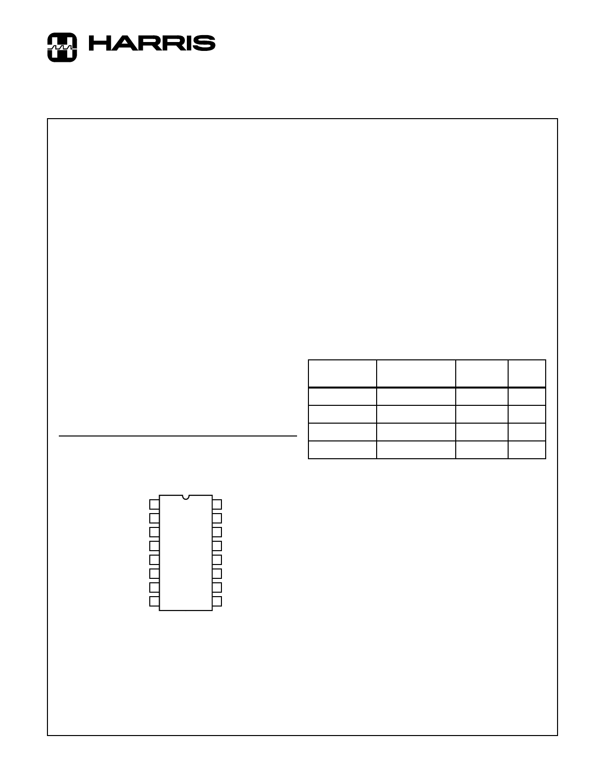
Pinout
CD74HC4094, CD74HCT4094
(PDIP, SOIC)
TOP VIEW
Description
The Harris CD74HC4094 and CD74HCT4094 are 8-stage
serial shift registers having a storage latch associated with
each stage for strobing data from the serial input to parallel
buffered three-state outputs. The parallel outputs may be
connected directly to common bus lines. Data is shifted on
positive clock transitions. The data in each shift register
stage is transferred to the storage register when the Strobe
input is high. Data in the storage register appears at the
outputs whenever the Output-Enable signal is high.
Two serial outputs are available for cascading a number of
these devices. Data is available at the QS
1
serial output
terminal on positive clock edges to allow for high-speed
operation in cascaded system in which the clock rise time is
fast. The same serial information, available at the QS
2
terminal on the next negative clock edge, provides a means
for cascading these devices when the clock rise time is slow.
14
15
16
9
13
12
11
10
1
2
3
4
5
7
6
8
STROBE
DATA
CP
Q
0
Q
1
Q
2
GND
Q
3
V
CC
Q
4
Q
5
Q
6
Q
7
QS
2
QS
1
OE
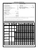
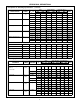
Ordering Information
PART NUMBER TEMP. RANGE (
o
C) PACKAGE
PKG.
NO.
CD74HC4094E -55 to 125 16 Ld PDIP E16.3
CD74HCT4094E -55 to 125 16 Ld PDIP E16.3
CD74HC4094M -55 to 125 16 Ld SOIC M16.15
CD74HCT4094M -55 to 125 16 Ld SOIC M16.15
NOTES:
1. When ordering, use the entire part number. Add the suffix 96 to
obtain the variant in the tape and reel.
2. Wafer or die for this part number is available which meets all elec-
trical specifications. Please contact your local sales office or
Harris customer service for ordering information.
November 1997
CAUTION: These devices are sensitive to electrostatic discharge. Users should follow proper IC Handling Procedures.
Copyright
© Harris Corporation 1997
File Number 1779.1
CD74HC4094,
CD74HCT4094
High Speed CMOS Logic
8-Stage Shift and Store Bus Register, Three-State