
Datasheet
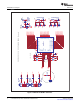
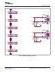
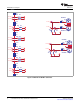
Table Of Contents
User's Guide
SCAU029 – May 2009
Low Additive Phase Noise Clock Buffer Evaluation Board
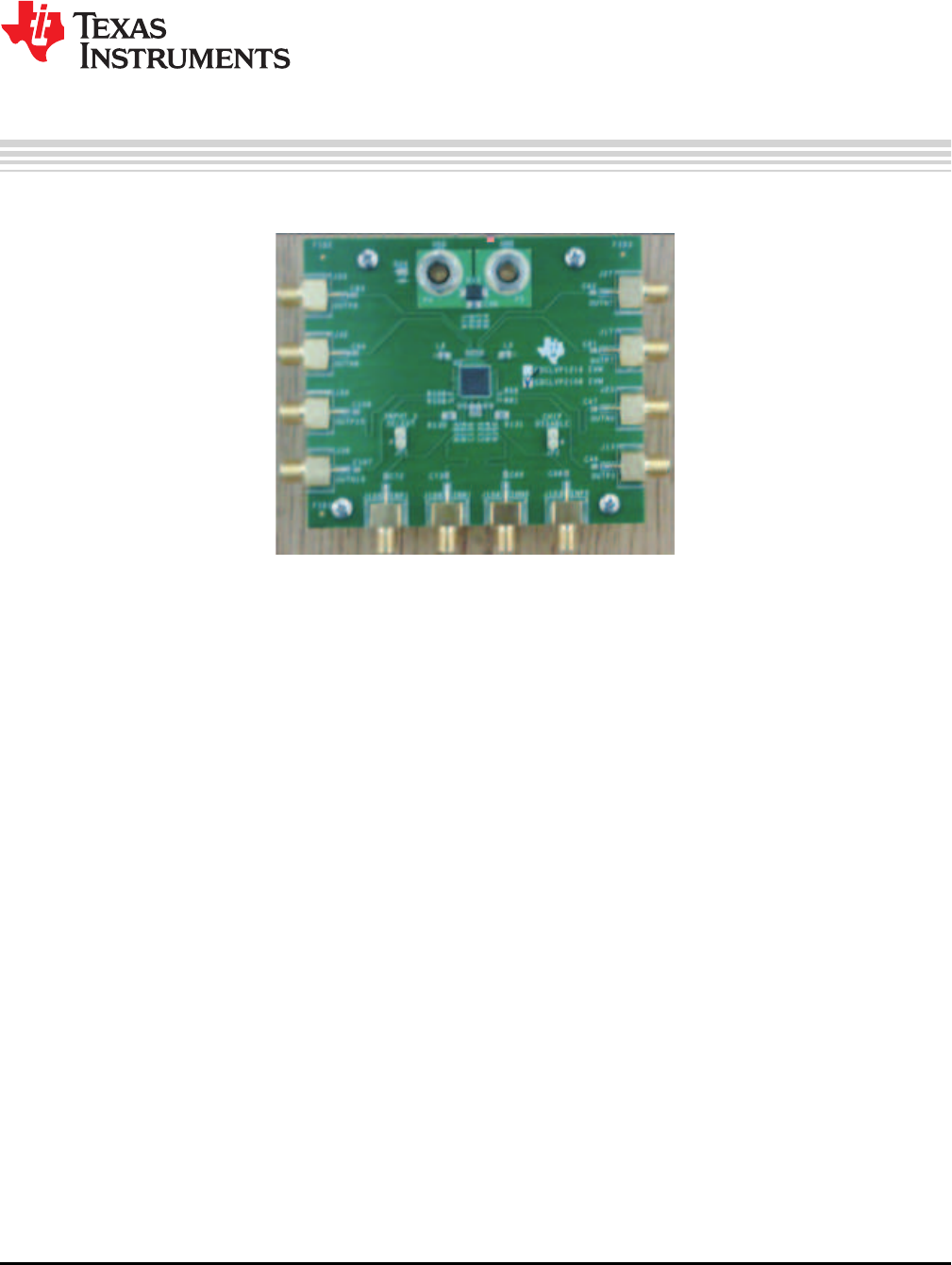
Figure 1. CDCLVP1216 Evaluation Board
Features:
• Easy-to-use evaluation board to fan out low phase noise clocks
• Easy device setup
• Fast configuration
• Control pins configurable through jumpers
• Board powered at +2.5-/+3.3-V
• Single-ended or differential input clocks
• CDCLVP1216 supports 16 LVPECL outputs; CDCLVP1216EVM supports four LVPECL outputs
Contents
1 General Description ......................................................................................................... 2
2 Signal Path and Control Circuitry .......................................................................................... 2
3 Getting Started ............................................................................................................... 2
4 Input Clock Selection ........................................................................................................ 2
5 Output Clock .................................................................................................................. 3
6 Schematics and Layout ..................................................................................................... 3
List of Figures
1 CDCLVP1216 Evaluation Board ........................................................................................... 1
2 CDCLVP1216EVM—Schematic ........................................................................................... 4
3 CDCLVP1216EVM—Schematic ........................................................................................... 5
4 CDCLVP1216EVM—Schematic ........................................................................................... 6
All trademarks are the property of their respective owners.
SCAU029 – May 2009 Low Additive Phase Noise Clock Buffer Evaluation Board 1
Submit Documentation Feedback