
Datasheet
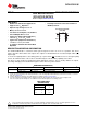
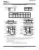


DCT OR DCU PACKAGE
(TOP VIEW)
1
2
3
4
8
7
6
5
1OE
1A
2Y
GND
V
CC
2OE
1Y
2A
SN74LVC2G125-Q1
www.ti.com
SCES559C –MARCH 2004– REVISED MARCH 2011
DUAL BUS BUFFER GATE
WITH 3-STATE OUTPUTS
Check for Samples: SN74LVC2G125-Q1
1
FEATURES
• Qualified for Automotive Applications • Latch-Up Performance Exceeds 100 mA Per
JESD 78, Class II
• Supports 5-V V
CC
Operation
• Inputs Accept Voltages to 5.5 V
• Max t
pd
of 4.3 ns at 3.3 V
• Low Power Consumption, 10-μA Max I
CC
• ±24-mA Output Drive at 3.3 V
• Typical V
OLP
(Output Ground Bounce)
<0.8 V at V
CC
= 3.3 V, T
A
= 25°C
• Typical V
OHV
(Output V
OH
Undershoot)
>2 V at V
CC
= 3.3 V, T
A
= 25°C
• I
off
Supports Partial-Power-Down Mode
Operation
DESCRIPTION/ORDERING INFORMATION
The SN74LVC2G125-Q1 is a dual bus buffer gate designed for 1.65-V to 5.5-V V
CC
operation. This device
features dual line drivers with 3-state outputs. The outputs are disabled when the associated output-enable (OE)
input is high.
To ensure the high-impedance state during power up or power down, OE should be tied to V
CC
through a pullup
resistor; the minimum value of the resistor is determined by the current-sinking capability of the driver.
This device is fully specified for partial-power-down applications using I
off
. The I
off
circuitry disables the outputs,
preventing damaging current backflow through the device when it is powered down.
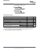
ORDERING INFORMATION
(1)
T
A
PACKAGE
(2)
ORDERABLE PART NUMBER TOP-SIDE MARKING
(3)
SSOP – DCT Tape and reel CLVC2G125IDCTRQ1 C25_ _ _
–40°C to 85°C
VSSOP – DCU Tape and reel CLVC2G125IDCURQ1 CCW_
(1) For the most current package and ordering information, see the Package Option Addendum at the end of this document, or see the TI
web site at www.ti.com.
(2) Package drawings, thermal data, and symbolization are available at www.ti.com/packaging.
(3) DCT: The actual top-side marking has three additional characters that designate the year, month, and assembly/test site.
DCU: The actual top-side marking has one additional character that designates the assembly/test site.
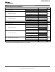
FUNCTION TABLE
(EACH BUFFER)
INPUTS
OUTPUT
Y
OE A
L H H
L L L
H X Z
1
Please be aware that an important notice concerning availability, standard warranty, and use in critical applications of Texas
Instruments semiconductor products and disclaimers thereto appears at the end of this data sheet.
PRODUCTION DATA information is current as of publication date.
Copyright © 2004–2011, Texas Instruments Incorporated
Products conform to specifications per the terms of the Texas
Instruments standard warranty. Production processing does not
necessarily include testing of all parameters.