
User manual

LCD Controller Operation
18-5LCD Controller
18.2.4 LCD Voltage Generation
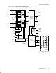
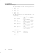
The voltages required for the LCD signals are supplied externally to pins R33,
R23, R13, and R03. Using an equally weighted resistor divider ladder between
these pins establishes the analog voltages as shown in Table 18−1. The
resistor value R is typically 680 kW. Values of R from 100kW to 1MW can be
used depending on LCD requirements.
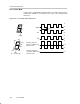
R33 is a switched-V
CC
output. This allows the power to the resistor ladder to
be turned off eliminating current consumption when the LCD is not used.
Table 18−1.External LCD Module Analog Voltage
OSCOFF LCDMXx LCDON VA VB VC VD R33
x xx 0 0 0 0 0 Off
1 xx x 0000Off
0 00 1 V5/V1 V1/V5 V5/V1 V1/V5 On
0 01 1 V5/V1 V1/V5 V3/V3 V1/V5 On
0
1x 1 V5/V1 V2/V4 V4/V2 V1/V5 On
LCD Contrast Control
LCD contrast can be controlled by the R03 voltage level with external circuitry,
typically an additional resistor Rx to GND. Increasing the voltage at R03
reduces the total applied segment voltage decreasing the LCD contrast.
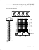
18.2.5 LCD Outputs
Some LCD segment, common, and Rxx functions are multiplexed with digital
I/O functions. These pins can function either as digital I/O or as LCD functions.
The pin functions for COMx and Rxx, when multiplexed with digital I/O, are
selected using the applicable PxSELx bits as described in the Digital I/O
chapter. The LCD segment functions, when multiplexed with digital I/O, are
selected using the LCDPx bits.
The LCDPx bits selects the LCD function for groups of pins. When LCDPx =
0, no multiplexed pin is set to LCD function. When
LCDPx = 1, segments S0 - S15 are selected as LCD function. When LCDPx
> 1, LCD segment functions are selected in groups of four. For example, when
LCDPx = 2, segments S0-S19 are selected as LCD function.
Note: LCDPx Bits Do Not Affect Dedicated LCD Segment Pins
The LCDPx bits only affect pins with multiplexed LCD segment functions and
digital I/O functions. Dedicated LCD segment pins are not affected by the
LCDPx bits.