
User manual

ADC12 Operation
20-9ADC12
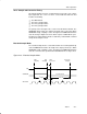
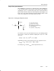
Sample Timing Considerations
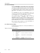
When SAMPCON = 0 all Ax inputs are high impedance. When SAMPCON =
1, the selected Ax input can be modeled as an RC low-pass filter during the
sampling time t
sample
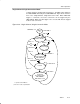
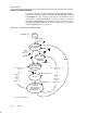
, as shown below in Figure 20−5. An internal MUX-on
input resistance R
I
(max. 2 kΩ) in series with capacitor C
I
(max. 40 pF) is seen
by the source. The capacitor C
I
voltage V
C
must be charged to within 1/2 LSB
of the source voltage V
S
for an accurate 12-bit conversion.
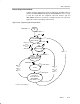
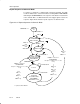
Figure 20−5. Analog Input Equivalent Circuit
R
S
R
I
V
S
V
C
MSP430
C
I
V
I
V
I
= Input voltage at pin Ax
V
S
= External source voltage
R
S
= External source resistance
R
I
= Internal MUX-on input resistance
C
I
= Input capacitance
V
C
= Capacitance-charging voltage
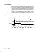
The resistance of the source R
S
and R
I
affect t
sample
. The following equation
can be used to calculate the minimum sampling time t
sample
for a 12-bit
conversion:
t
sample
u (R
S
) R
I
) ln(2
13
) C
I
) 800ns
Substituting the values for R
I
and C
I
given above, the equation becomes:
t
sample
u (R
S
) 2kW) 9.011 40pF ) 800ns
For example, if R
S
is 10 kΩ, t
sample
must be greater than 5.13 µs.