
User manual

ADC12 Operation
20-17ADC12
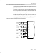
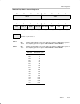
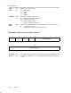
20.2.9 ADC12 Grounding and Noise Considerations
As with any high-resolution ADC, appropriate printed-circuit-board layout and
grounding techniques should be followed to eliminate ground loops, unwanted
parasitic effects, and noise.
Ground loops are formed when return current from the A/D flows through paths
that are common with other analog or digital circuitry. If care is not taken, this
current can generate small, unwanted offset voltages that can add to or
subtract from the reference or input voltages of the A/D converter. The
connections shown in Figure 20−11 help avoid this.
In addition to grounding, ripple and noise spikes on the power supply lines due
to digital switching or switching power supplies can corrupt the conversion
result. A noise-free design using separate analog and digital ground planes
with a single-point connection is recommend to achieve high accuracy.
Figure 20−11.ADC12 Grounding and Noise Considerations
DV
CC
DV
SS
AV
CC
AV
SS
Ve
REF+
Digital
Power Supply
Decoupling
10 uF 100 nF
+
Using an External
Positive
Reference
V
REF+
V
REF−
/ Ve
REF−
Using the Internal
Reference
Generator
10 uF 100 nF
100 nF
+
+
10 uF 100 nF
+
Using an External
Negative
Reference
10 uF
+
Analog
Power Supply
Decoupling
10 uF 100 nF