
User manual


9.9 Clock and Oscillator Control
9.10 System Control Register Descriptions
www.ti.com
Clock and Oscillator Control
The auxiliary (24 MHz) oscillator and the clock source of the CLKOUT, AUDIO_CLK0, and AUDIO_CLK1
outputs are controlled by the clock and oscillator control register (CLKCTL). See the device-specific data
manual for details on CLKCTL.
Table 9-3 lists the memory-mapped registers for the system control. See the device-specific data manual
for the memory address of these registers and complete descriptions.
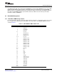
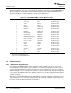
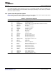
Table 9-3. System Control Registers
Offset Acronym Register Description
0h PINMUX0 Pin Multiplexing Control 0
4h PINMUX1 Pin Multiplexing Control 1
8h DSPBOOTADDR DSP Boot Address. Decoded by bootloader software for host boots.
Ch SUSPSRC Emulator Suspend Source
10h BOOTSTAT Boot Status
14h BOOTCFG Device Boot Configuration
24h ARMBOOT ARM926 Boot Control
28h JTAGID Device ID Number
30h HPICTL HPI Control
34h USBCTL USB Control
38h VIDCLKCTL Video Clock Control
3Ch MSTPRI0 Bus Master Priority Control 0
40h MSTPRI1 Bus Master Priority Control 1
44h MSTPRI2 Bus Master Priority Control 2
48h VDD3P3V_PWDN V
DD
3.3-V I/O Powerdown Control
50h TSIFCTL TSIF Control
54h PWMCTL PWM Control
58h EDMATCCFG EDMA TC Configuration
5Ch CLKCTL Oscillator and Output Clock Control
60h DSPINT ARM to DSP Interrupt Status
64h DSPINTSET ARM to DSP Interrupt Set
68h DSPINTCLR ARM to DSP Interrupt Clear
6Ch VSCLKDIS Video and TSIF Clock Disable
70h ARMINT DSP to ARM Interrupt Status
74h ARMINTSET DSP to ARM Interrupt Set
78h ARMINTCLR DSP to ARM Interrupt Clear
7Ch ARMWAIT ARM Memory Wait State Control
SPRUEP9A – May 2008 System Control Module 109
Submit Documentation Feedback