
Datasheet
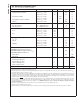

Absolute Maximum Ratings (Note 10)
If Military/Aerospace specified devices are required,
please contact the National Semiconductor Sales Office/
Distributors for availability and specifications.
Supply Voltage (V
CC
)7V
Voltage at Any Pin −0.6V to V
CC
+0.6V
ESD Protection Level 2 kV
(Human Body Model)
Total Current into V
CC
Pin (Source) 80 mA
Total Current out of GND Pin (Sink) 100 mA
Storage Temperature Range −65˚C to +140˚C
Note 10:
Absolute maximum ratings indicate limits beyond which damage to
the device may occur. DC and AC electrical specifications are not ensured
when operating the device at absolute maximum ratings.
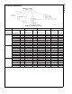
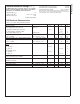
DC Electrical Characteristics
−40˚C ≤ T
A
≤ +85˚C unless otherwise specified.
Parameter Conditions Min Typ Max Units
Operating Voltage 2.7 5.5 V
Power Supply Rise Time from 0.0V (Note 17)
(On-Chip Power-On Reset Selected) 10 ns 50 ms
V
CC
Start Voltage to Guarantee POR 0.25 V
Power Supply Ripple (Note 12) Peak-to-Peak 0.1 V
CC
V
Supply Current (Note 13)
CKI = 10 MHz V
CC
= 5.5V, t
C
= 1 µs 6.0 mA
HALT Current (Note 14) —WATCHDOG Disabled V
CC
= 5.5V, CKI = 0 MHz
<
4 10.0 µA
IDLE Current (Note 13)
CKI = 10 MHz V
CC
= 5.5V, t
C
= 1 µs 1.5 mA
Input Levels (V
IH
,V
IL
)
RESET
Logic High 0.8 V
CC
V
Logic Low 0.2 V
CC
V
CKI, All Other Inputs
Logic High 0.7 V
CC
V
Logic Low 0.2 V
CC
V
Value of the Internal Bias Resistor 0.5 1.0 2.0 MΩ
for the Crystal/Resonator Oscillator
CKI Resistance to V
CC
or GND when R/C V
CC
= 5.5V 5 8 11 kΩ
Oscillator is Selected
Hi-Z Input Leakage (same as TRI-STATE output) V
CC
= 5.5V −2 +2 µA
Input Pullup Current V
CC
= 5.5V, V
IN
= 0V −40 −250 µA
G and L Port Input Hysteresis 0.25 V
CC
V
COP8SA Family
www.national.com9