
Datasheet

COP8SGE5, COP8SGE7, COP8SGH5
COP8SGK5, COP8SGR5, COP8SGR7
SNOS516E –JANUARY 2000–REVISED APRIL 2013
www.ti.com
NOTE
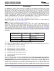
Care must be exercised with the D2 pin operation. At RESET, the external loads on this
pin must ensure that the output voltages stay above 0.7 V
CC
to prevent the chip from
entering special modes. Also keep the external loading on D2 to less than 1000 pF.
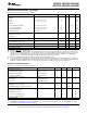
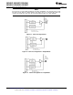
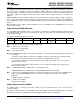
Figure 13. I/O Port Configurations
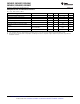
Figure 14. I/O Port Configurations—Output Mode
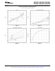
Figure 15. I/O Port Configurations—Input Mode
16 Submit Documentation Feedback Copyright © 2000–2013, Texas Instruments Incorporated
Product Folder Links: COP8SGE5 COP8SGE7 COP8SGH5 COP8SGK5 COP8SGR5 COP8SGR7