
Datasheet


COP8SGE5, COP8SGE7, COP8SGH5
COP8SGK5, COP8SGR5, COP8SGR7
SNOS516E –JANUARY 2000–REVISED APRIL 2013
www.ti.com
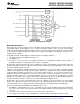
F2 Comparator1 positive input
F1 Comparator1 negative input
A Comparator Select Register (CMPSL) is used to enable the comparators, read the outputs of the comparators
internally, and enable the outputs of the comparators to the pins. Two control bits (enable and output enable) and
one result bit are associated with each comparator. The comparator result bits (CMP1RD and CMP2RD) are
read only bits which will read as zero if the associated comparator is not enabled. The Comparator Select
Register is cleared with reset, resulting in the comparators being disabled. The comparators should also be
disabled before entering either the HALT or IDLE modes in order to save power. The configuration of the CMPSL
register is as follows:
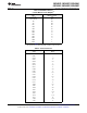
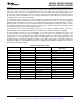
CMPSL REGISTER (ADDRESS X'00B7)
Reserved CMP20E CMP2RD CMP2EN CMP10E CMP1RD CMP1EN Reserved
Bit 7 Bit 0
The CMPSL register contains the following bits:
Reserved These bits are reserved and must be zero
CMP20E Selects pin I6 as comparator 2 output provided that CMP2EN is set to enable the comparator
CMP2RD Comparator 2 result (this is a read only bit, which will read as 0 if the comparator is not enabled)
CMP2EN Enable comparator 2
CMP10E Selects pin I3 as comparator 1 output provided that CMPIEN is set to enable the comparator
CMP1RD Comparator 1 result (this is a read only bit, which will read as 0 if the comparator is not enabled)
CMP1EN Enable comparator 1
Note that the two unused bits of CMPSL may be used as software flags.
Note: If the user attempts to use the comparator output immediately after enabling the comparator, an incorrect
value may be read. At least one instruction cycle should pass between these operations. The use of a direct
addressing mode instruction for either of these two operations will ensure this delay in the software.
NOTE
For compatibility with existing code and with existing Mask ROMMed devices the bits of
the CMPSL register will take precedence over the associated Port F configuration and
data output bits.
Interrupts
INTRODUCTION
Each device supports thirteen vectored interrupts. Interrupt sources include Timer 0, Timer 1, Timer 2, Timer 3,
Port L Wakeup, Software Trap, MICROWIRE/PLUS, and External Input.
All interrupts force a branch to location 00FF Hex in program memory. The VIS instruction may be used to vector
to the appropriate service routine from location 00FF Hex.
The Software trap has the highest priority while the default VIS has the lowest priority.
Each of the 13 maskable inputs has a fixed arbitration ranking and vector.
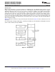
Figure 34 shows the Interrupt Block Diagram.
44 Submit Documentation Feedback Copyright © 2000–2013, Texas Instruments Incorporated
Product Folder Links: COP8SGE5 COP8SGE7 COP8SGH5 COP8SGK5 COP8SGR5 COP8SGR7