
Datasheet


COP8SGE5, COP8SGE7, COP8SGH5
COP8SGK5, COP8SGR5, COP8SGR7
www.ti.com
SNOS516E –JANUARY 2000–REVISED APRIL 2013
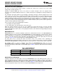
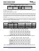
Figure 40. MICROWIRE/PLUS SPI Mode Interface Timing, Normal SK Mode, SK Idle Phase being High
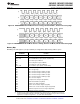
Figure 41. MICROWIRE/PLUS SPI Mode Interface Timing, Alternate SK Mode, SK Idle Phase being High
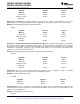
Memory Map
All RAM, ports and registers (except A and PC) are mapped into data memory address space.
Address
Contents
(1)
S/ADD REG
0000 to 006F On-Chip RAM bytes (112 bytes)
0070 to 007F Unused RAM Address Space (Reads As All Ones)
xx80 to xx93 Unused RAM Address Space (Reads Undefined Data)
xx94 Port F data register, PORTFD
xx95 Port F configuration register, PORTFC
xx96 Port F input pins (read only), PORTFP
xx97 to xxAF Unused address space (Reads Undefined Data)
xxB0 Timer T3 Lower Byte
xxB1 Timer T3 Upper Byte
xxB2 Timer T3 Autoload Register T3RA Lower Byte
xxB3 Timer T3 Autoload Register T3RA Upper Byte
xxB4 Timer T3 Autoload Register T3RB Lower Byte
xxB5 Timer T3 Autoload Register T3RB Upper Byte
xxB6 Timer T3 Control Register
xxB7 Comparator Select Register (Reg:CMPSL)
xxB8 UART Transmit Buffer (Reg:TBUF)
xxB9 UART Receive Buffer (Reg:RBUF)
xxBA UART Control and Status Register (Reg:ENU)
xxBB UART Receive Control and Status Register (Reg:ENUR)
xxBC UART Interrupt and Clock Source Register (Reg:ENUI)
xxBD UART Baud Register (Reg:BAUD)
(1) Reading memory locations 0070H–007FH (Segment 0) will return all ones. Reading unused memory
locations 0080H–0093H (Segment 0) will return undefined data. Reading memory locations from other
Segments (i.e., Segment 4, Segment 5, … etc.) will return undefined data.
Copyright © 2000–2013, Texas Instruments Incorporated Submit Documentation Feedback 57
Product Folder Links: COP8SGE5 COP8SGE7 COP8SGH5 COP8SGK5 COP8SGR5 COP8SGR7